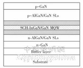
1 Introduction Light emitting diodes (LEDs) are an important solid-state light source with low cost and long life. The GaN-based material has a forbidden band width of 0.7 to 6. 2 eV, and its illuminating wavelength can range from 650 nm to 200 nm, enabling full spectrum from infrared light, red light, green light, blue light, and ultraviolet light. Luminous, with broad application prospects and huge market potential. Intrinsic point defects such as lattice vacancies, interstitial atoms and anti-position defects generated inside the LED [1] have a great influence on the electrical properties and optical properties of materials and devices. Electron beam irradiation is an important means to study the point defects in materials [2]. GaN has strong anti-irradiation characteristics, so it is an important research content to further improve the anti-irradiation characteristics of GaN-based light-emitting devices through process improvement and optimization. There have been related experimental reports on electron beam irradiation of GaN material LEDs at home and abroad [3-5]. In 1999, ZQ Fang et al found that 1 MeV electron irradiation can induce deep levels (Ec≈0. 18 eV) in GaN materials. In 2002, Gelhausen et al. [6] also used low-energy electron irradiation to study the defects of Mg-doped GaN-based LEDs, improved the luminous efficiency of the device, and studied its mechanism. In 2003, Shar- Shar et al. [7] pointed out that in the study of the electron irradiation and gamma irradiation effects of LEDs, the low-dose electron irradiation increased the brightness of the LED normalized from 16% to 54%, and began to degrade at high doses. . In this paper, GaN material LEDs are irradiated by electron beams with different energies, and the luminescence properties of LEDs are studied by PL spectra. The irradiation energy is combined with the change of the optical properties of the GaN material LED, and the electron beam irradiation mechanism of different energies is studied by the luminescence characteristics. 2 experiment The structure of the GaN material selected in the experiment is shown in Figure 1. The experimental samples were divided into GaN-based LED epitaxial wafers 1# and 2#. The two epitaxial wafers have the same structure and different growth parameters. Irradiation experiments were carried out using Dynamitron series accelerators for different energy and dose electron beam irradiation experiments under standard atmospheric pressure, normal air atmosphere and ambient temperature irradiation atmosphere. The electron beam irradiation of 1. 5 MeV was performed on the 1# epitaxial wafer, and the radiation dose was 10 kGy and 100 kGy; the 3# epitaxial wafer was irradiated with 3 MeV and 4.5 MeV respectively, and the irradiated LED was irradiated. The epitaxial wafer was subjected to a room temperature PL spectrum test. Figure 1 Schematic diagram of GaN-based LED material structure 3 Results and discussion 3.1 1.5 MeV electron beam irradiation LED PL spectrum test For the GaN-based LED epitaxial wafer 1#, an electron beam irradiation of 1.5 MeV was performed, and the irradiation doses were 10 kGy and 100 kGy, respectively, and the PL spectrum test was performed to obtain the luminescence properties of the GaN-based LED. Figure 2 PL spectrum of GaN-based LED after 1.5 MeV electron beam irradiation The curve (a) in Fig. 2 is the PL spectrum of the unirradiated 1# GaN epitaxial wafer, and the curves (b) and (c) are the PL spectra after 10 kGy and 100 kGy electron beam irradiation, respectively. As can be seen from the figure, the 1# chip has a dominant wavelength of about 460 nm and a small luminescence peak at 425 nm. The small luminescence peak at 425 nm is generated by the energy level transition from the deep level defect group under the conduction band to the forbidden band. The main luminescence peak is the band gap transition of InGaN/GaN (around 430 nm) and quantum wells. The red shift caused by the Tok effect is caused jointly. When an electron bombards a semiconductor material, a hole-interval atom pair is formed due to the interaction of the irradiated electron with the material lattice, destroying the position of the crystal lattice. These vacancies will further interact with impurities or other vacancies to form more complex defects, which in turn form new electronic energy levels in the forbidden band. Both the electron and hole trapping cross sections and the energy level density contribute to the recombination of the unbalanced carriers, resulting in a decrease in minority carrier lifetime and carrier concentration. The relationship between the minority carrier lifetime τ and the irradiation dose can be expressed as follows: Where τ0 is the lifetime of the minority before irradiation, k is the radiation damage coefficient, and n is the irradiation dose. At lower doses, as the irradiation dose increases, the minority carrier lifetime decreases and the diffusion length decreases, creating a narrow intrinsic region near the pn junction. The generation of the intrinsic region will cause a significant increase in the forward current while causing an increase in the luminous intensity. At higher doses, the electron concentration nt(t) of the defect capture can be expressed as follows: Where Nt0 is the intrinsic concentration of the defect, T is the system temperature, αrate is the heating rate constant, τann is the carrier annihilation time, and τe is the carrier generation time. It can be seen from equation (2) that as the lifetime of the minority carrier is shortened, the minority carrier concentration of the defect capture is also reduced, and the composite probability is decreased, causing the luminescence intensity to decrease. The effect of irradiation on the dominant wavelength can also be seen in Figure 2. After irradiation with 10 kGy and 100 kGy electron beams, the position of the luminescence peak of the epitaxial wafer changes little, and red shift occurs at small doses, and blue shift occurs at high doses. The red shift occurs at low doses because when the low-dose electron beam irradiates the LED, the deep level defects generated inside the material are mainly used to compensate for the lack of chemical doping, so that the Fermi level is far from the bottom of the conduction band. Resulting in a reduction in the forbidden band width of the material; a blue shift occurs when the dose is increased, and it can be considered that the interaction force between the atoms in the GaN material changes due to a large number of defects generated by the irradiation in the material, thereby causing the forbidden band width of the material. increase. The intensity of the LED luminescence peak has also changed. At 10 kGy doses, the luminous intensity of the LED increases by about 25%; while at 100 kGy, the luminous intensity of the LED decreases by about 16%.