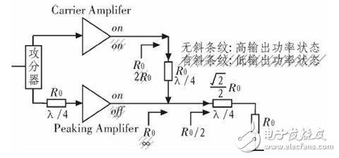
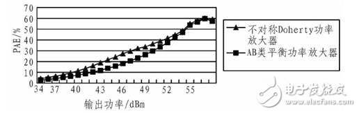
For modern wireless communication systems, multi-carrier, broadband, and high transmission rates have become the development direction. With the increasing strain of spectrum resources, in order to transmit more data in a limited bandwidth, nonlinear modulation methods such as BPSK and QPSK are adopted in WCDMA systems, and the instantaneous transmission power of the system generates a high peak-to-average ratio, and the power amplifier needs The system's linearity requirements are met by a large power backoff. At present, power amplifiers in WCDMA base stations or repeaters are the most important power consumption units. In order to meet the linearity requirements of the system, they are usually biased in Class A and Class AB, and the efficiency is relatively low, generally 8% to 15%. Research and design of linear and efficient RF power amplifiers has become a hot topic in the research field of power amplifiers. The power amplifiers of the Doberty structure have attracted more and more attention and research because of their high efficiency, simple implementation method and low cost. Based on the ADS simulation platform, based on the in-depth study and analysis of the working principle and advantages and disadvantages of the Doherty structure, this paper designs an asymmetric Doberty power amplifier that satisfies the performance requirements of WCDMA base stations. 1.1 How does the traditional Doberty power amplifier work? The schematic diagram of the traditional Doberty power amplifier is shown in Figure 1. It is generally composed of a carrier amplifier (Carrier Amplifier) ​​and a peak amplifier (PeakingAmplifier) ​​connected in parallel. The carrier amplifier is generally biased in the AB mode, and the output is connected in series with a microstrip line to perform impedance transformation; the peak amplifier is generally biased in the C mode, and the input microstrip line at the front end of the matching network is phase balanced. effect. Figure 1 Schematic diagram of the structure of a traditional Doberty power amplifier As can be seen from Figure 1, the power amplifier of the conventional Doberty structure has two operating states: a low output power state (with diagonal stripes in Figure 1) and a high output power state (no diagonal stripes in Figure 1). In the high output power state, ideally, the output currents of the two amplifiers are equal, and the carrier amplifier and the peak amplifier produce equal output operations. At this time, the load impedance of the carrier amplifier and the peak amplifier are both R0, and normally R0=50Ω. In the low output power state, the peak amplifier cutoff does not work and only the carrier amplifier is turned on. Theoretically, the output impedance of the peak amplifier tends to infinity at this time, and the influence of the peak amplifier on the impedance of the load network can be neglected. The load impedance at the output of the carrier amplifier is converted to 2R0 by the λ/4 microstrip line of R0 with characteristic impedance, which enables high load impedance to achieve efficiency improvement at low output power. At this time, the saturated output power of the carrier amplifier is four times smaller than the total peak output power, that is, the saturated output power of the conventional Doherty power amplifier in the low output power region is 6 dB lower than the peak saturation output, thereby achieving early saturation. Purpose to improve efficiency when power is backed up. 1.2 Basic theory of asymmetric Doherty power amplifier In traditional Doherty-structured power amplifiers, the carrier amplifier is biased in class AB, while the peaking amplifier is typically biased in class C. When the input signal is the same, the peak amplifier current must be lower than the carrier amplifier current. When the output power is saturated, since the output voltages of the two amplifiers are equal, the output power of the peak amplifier is necessarily smaller than the output power of the carrier amplifier, which is different from the ideal case. According to the active load traction theory, when the peak amplifier current does not reach the ideal value, it will inevitably lead to insufficient traction of the peak amplifier to the carrier amplifier, so that the output impedance of the carrier amplifier changes from high impedance 100Ω to 50 Ω low impedance. No traction to 50 Ω ultimately affects the performance of the Doherty power amplifier. Asymmetric Doherty power amplifiers are based on traditional Doherty power amplifiers. They are generally implemented with asymmetric power drivers and different power amplifier tubes. Compared with the implementation method using different power amplifier tubes, the asymmetric power driving scheme is relatively simple in structure and easy to implement. For asymmetric Doherty power amplifiers, in low output power states, the carrier amplifier is biased in class AB, the peak amplifier is turned off, and the linearity of the power amplifier is primarily dependent on the carrier amplifier. In the high output power state, the linearity of the asymmetric Doherty power amplifier can optimize IMD3 performance by adjusting the gate bias of the two power amplifier tubes. Therefore, in the design, the input power distribution ratio and the gate bias voltage of the carrier amplifier and the peak amplifier can be constantly adjusted, so that the designed asymmetric power amplifier has the best performance. In the following sections, based on the ADS simulation platform, Freescale's MRF6S21140H power amplifier tube is used to design an asymmetric power-driven Doherty power amplifier for WCDMA base stations operating in the 2.14 GHz band. In the simulation design, the ADS platform can simplify the design steps and shorten the development cycle. The MRF6S21140H power amplifier tube model used in the simulation design is a semi-empirical model provided by Freescale. In the simulation design, the static working point and steady state of the transistor are determined by simulation analysis of the DC bias and stability of the transistor. Using the load pull and source traction simulation in ADS, the equal power circle and the equal efficiency circle of different impedance values ​​of the transistor are obtained, and the optimal impedance value suitable for the asymmetric Doherty power amplifier is obtained, and the optimized impedance is applied in the bias circuit. The method reduces the electrical memory effect better. By comprehensively considering the design idea of ​​the compensation network in the matching network and designing the compensation line, the power leakage of the asymmetric Doherty power amplifier is more effectively suppressed, and the output efficiency is improved. After completing the simulation design of each module of the asymmetric Doherty power amplifier, the input microstrip line is adjusted to align the phase of the output signals of the two branches of the carrier amplifier and the peak amplifier, and the asymmetry of the design is optimized by the schematic-layout joint simulation. The performance of the power amplifier improves the accuracy of the simulation and narrows the gap between simulation and practical applications. Simultaneously comparing the power distribution ratio and gate bias voltage simulation results of different input power splitters, it is found that when the carrier amplifier has a gate bias voltage of 2.84V and the peak amplifier has a gate bias voltage of 0.85V, When the drain bias voltage is 28V, the performance of the asymmetric Doherty power amplifier with a power distribution ratio of 1:2.3 at the input power splitter is optimal. Figure 2 is a graph comparing the power-added efficiency (PAE) of a 1:2.3 asymmetric power-driven Doherty power amplifier with a Class AB balanced power amplifier. It can be seen from Fig. 2 that the peak saturated output power is about 55.8 dBm, so the asymmetric structure can improve the mismatch problem caused by the peak amplifier's insufficient traction of the carrier amplifier, so that the saturated output power of the bee is ideal. When the output power is 11.8dB, the output power is 44dBm. The 1:2.3 asymmetric power-driven Doherty power amplifier PAE is 24.21%, and the PAE of the AB balanced power amplifier is 15.63%. Therefore 1: 2.3 Asymmetric power-driven Doherty power amplifiers have an 8.58% increase in PAE over Class AB balanced power amplifiers. Figure 2 PAE comparison curve of asymmetric Doherty power amplifier and AB balanced power amplifier Cell Phone Case, Mobile Phone Covers, Clear Phone Case, Mobile Phone Case, TPU Phone Case, Silicone Phone Case Shenzhen Jianjiantong Technology Co., Ltd. , https://www.jonsun-sz.com