Fixed Optical Attenuator refers to the attenuator that can reduce the power of fiber light at a fixed value loss. A series of variable Fiber Optic Attenuator include SC ,FC, LC, ST, MU, SC/APC ,FC/APC fiber attenautor.Fixed Optical Attenuator can be female to female which is called bulkhead fiber fixed optical attenuator or male to female which is also called a plug fiber optic attenuator. Bulkhead and plug types are designed without cables. Foclink,a reliable supplier of fixed optical attenuator is always beside u 7*24. Fixed Optical Attenuator Fixed Optical Attenuator,Fixed Attenuator,Mini Fixed Optical Attenuator Foclink Co., Ltd , https://www.scfiberpigtail.com
Overview In many launch applications, multiple analog outputs with accurately known relative phases must be generated. In a quadrature modulator (Figure 1), the I and Q channels must have a clear phase relationship to achieve image frequency suppression. In Figure 1, the delays of DAC1 and DAC2 must match. Transmitters using digital beamforming technology need to accurately control the relative phase between a large number of DACs. 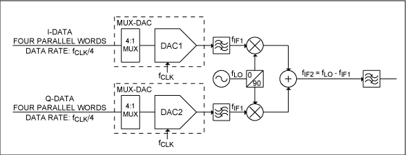
Figure 1. DAC and first up-conversion stage in I / Q transmitter using multiplexed DAC
When using a DAC with multiple inputs (MUX-DAC) such as the MAX19692, or an interpolated DAC with a data clock output, the input data rate is 1 / N of the DAC refresh rate, and the DAC locks on one or two data clock transition edges Save the data. In MAX19692, N = 4 and the input data rate is 1/4 of the DAC refresh rate. The DAC outputs a data clock (DATACLK) obtained by digitally dividing the input clock. When the DAC is powered on, the digital clock divider can be started in any of the N states. If multiple DACs are used, the clock dividers of different DACs will start in different states, so the DAC will latch the data at different times. Unless this situation is discovered and corrected, different DACs may output data with a delay of one or more clock cycles from each other. If the clock divider of each DAC can be reset, then this situation can be avoided, but there will still be some problems. If an error occurs in one of the clock dividers, the DAC will become permanently out of phase unless some error state detection method is performed. In order to ensure the reliability of the system, the phase error state must be detected and corrected. If the DAC is operating at a very high speed, the synchronization of the reset signal and the input clock may also be a problem.
Figure 2 shows a simplified block diagram of the MAX19692 clock (CLKP, CLKN) and data clock (DATACLKP, DATACLKN) interface. The initial clock is divided by a two-bit counter divided by four to latch the digital DAC input. The counter may be started in any of the four states (Figure 3). If two multiplexed DACs are used, the two DACs may start in different states. This may cause a delay of -1, 0, 1, or 2 clock cycles between the latch of DAC1 and the latch of DAC2.
The data clock output of MAX19692 is divided by 2 or 4 by the data input latch clock. The data is then latched at the two transition edges of the clock in double data rate (DDR) mode, or at every 90 ° phase of the clock in quad data rate (QDR) mode. If the data clock delays of multiple DACs match, or the data clocks are inverted from each other, then the latch clocks match. 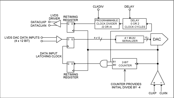
Figure 2. MAX19692 internal clock interface block diagram 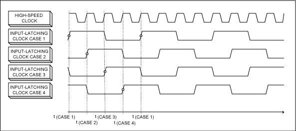
Figure 3. The MAX19692 latched clock (four possible states)
There are two aspects to the DAC synchronization problem: The relative phase between the DAC's latched clocks must be detected. The relative phase between the DACs must be adjusted until the DACs are properly phased. Detecting the phase error between DACs can be achieved by detecting the phase error of the data clock output between the two DACs. The phase detector can be as simple as an XOR gate, or it can be as complex as a phase frequency detector.
The phase adjustment between the two DACs can be achieved by operating the clock of one or more DACs until the relative phase of the DAC data clock output is zero. Another method can measure the number of DAC delay cycles between data clocks and the corresponding delay data. The following paragraphs describe these two methods in I / Q configuration.
DAC phase adjustment by "swallowing" pulses If the DAC uses a square wave (such as ECL) clock, the synchronization between the two DACs can be achieved using the simple high-speed logic circuit shown in Figure 4. For simplicity, the logic configuration in this schematic can only achieve single-ended functions. But in practical applications, differential logic such as ECL will be used to achieve high speed and low noise performance. 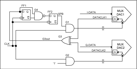
Figure 4. Simple high-speed logic circuit for DAC synchronization
The insertion of an AND gate (G1) in the clock path of MUX-DAC1 allows operation of the clock of MUX-DAC1. AND gate (G2) is inserted in the clock path of MUX-DAC2 for delay matching. The XOR gate (G3) plays the role of phase detection. When the outputs of DATACLK1 and DATACLK2 are different, G3 outputs "1". If G3out = "1", the clock pulse of MUX-DAC1 should be "swallowed", shifting the edge of DATACLK1 by one CLK clock cycle. The rising edge of G3 output (G3out) is detected by the rising edge detector (PED) composed of FF1 and G4. If a rising edge is detected, PED outputs "0" for one clock cycle. Before SPB is applied to G1, FF2 retimes this signal so that a clock pulse of MUX-DAC1 is suppressed. This delays DATACLK1 by one CLK clock cycle. After several clock cycles, the delay of DATACLK1 is consistent with DATACLK2, as shown in Figure 5. When using this method, the flip-flop must update the state on the falling edge of the clock to eliminate the glitch of the DAC clock signal. The input timing of the two MUX-DACs must be the same. When routing, consider the delay to ensure that the setup and hold times of the two flip-flops are met, and apply the pulse of the SPB signal to G1 when the clock is low. Otherwise, the clock signal may generate glitches. It is also recommended to use a noise-free power supply for the clock synchronization circuit to minimize the introduction of jitter. 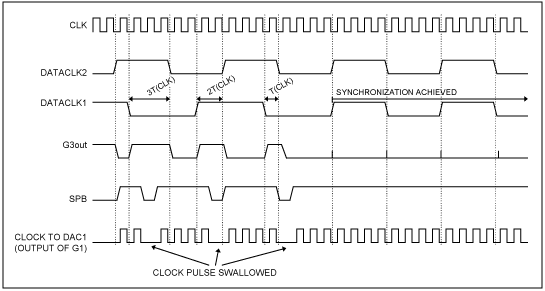
Figure 5. Timing diagram of the operation of the logic circuit shown
The DAC phase adjustment through input data shift can utilize the advanced digital clock management program (DCM) in Xilinx® FPGA to detect the phase difference between the data clocks of the two MUX-DACs (Figure 6). DCM1 generates a clock with the same frequency as DATACLK1 and DATACLK2. The delay of DCLK1 is dynamically adjusted at a pitch of 1/256 of the clock period. The flip-flops DFF1 and DFF2 sample DATACLK1 and DATACLK2 once every clock cycle. If DFF1 samples DATACLK1 when DATACLK1 is low, DFF1 will output a fixed "0". If DFF1 samples DATACLK1 when DATACLK1 is high, DFF1 will output a fixed "1". So DFF3 and DFF4 can be clocked at any clock phase, regardless of the delay setting of DCLK1. By grading the delay of DCLK1, using the dynamic delay adjustment function of DCM1 and reading the outputs of DFF3 and DFF4, we can get the delay setting based on the rising edges of DATACLK1 and DATACLK2. According to the delay setting, we can calculate the number of DAC clock cycles that the input data of MUX-DAC1 needs to be delayed in order to keep the input data of MUX-DAC1 and MUX-DAC2 in phase. The implementation of the 4 x 4 barrel shifter in FPGA allows the data latency to be changed in increments of one DAC clock cycle (see Figure 6).
MAX19692 has four parallel data ports A, B, C, and D. The data sequence input to the DAC is An, Bn, Cn, Dn, An + 1, Bn + 1, Cn + 1, Dn + 1, An + 2, etc. The 12-bit 4 x 4 cylindrical shifter (Figure 6) allows data input to MUX-DAC1 to be delayed by -1, 0, 1, or 2 CLK cycles. Therefore, the data latency can be adjusted until the output data of the two DACs are in phase. In this case, the data clocks of the two DACs may be separated by several integer clock (CLK) cycles and no longer change. Since the setup and hold time of the DAC is based on the data clock, the data timing of the two DACs must be different. This can be achieved by driving multiple DCMs in the FPGA of the DAC. 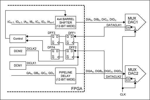
Figure 6. Using the barrel shifter implementation in FPGA to complete MUX-DAC synchronization
Each DAC uses a PLL to achieve DAC synchronization. If the DAC uses a phase-locked loop (PLL) synthesizer for timing, the method of synchronizing the two DACs is to use a separate PLL for each DAC (Figure 7). The LVDS data clock output phase of DAC1 and DAC2 is compared with the reference clock. In this case, the internal clock divider of the DAC is used as the feedback divider in the clock generation PLL. 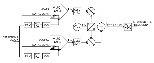
Figure 7. Each DAC uses a PLL for MUX-DAC synchronization
In this method, the setup and hold times of the two DACs match. But this method has two disadvantages. Two PLLs will bring extra cost and the phase noise limit of PLL may cause performance limit.
Conclusion MAX19692 is a 2.3Gsps, 12-bit DAC that can work in multiple Nyquist bands. It has an integrated 4: 1 input data multiplexer and is an ideal device for I / Q applications. When the use of MAX19692 in I / Q applications is emphasized, the solution discussed is equally applicable to other DACs and applications, such as the MAX5858A used in more than two channel applications. The scheme recommended in this article is applicable to any number of DACs. In order to properly synchronize high-speed devices, the delay associated with the board leads must also be considered.
Synchronization of multiple high-speed, multiplexed DACs in launch applications
Abstract: This application note provides synchronization methods for multiple high-speed multiplexed digital-to-analog converters (DACs) with multiple inputs or integrated interpolation filters. Such DACs are used in I / Q upconverters or digital beamforming transmitters. These DACs can provide data clock output for synchronization with the data source.