modern led crystal Table Lamp, with stainless steel and Top K9 crystals materials and unique designs, they are very popular in modern style rooms. It use the led light source which is energy saving and eye protecting. Modern crystal table lamp has many unique style and apperance.Its function is to focus the light in a small area, easy to work and study. Decorative table
lamp appearance of luxury, material and style and diverse, light
structure is complex, for the decorative effect of space, decorative and
lighting functions as important.
Modern Crystal Table Light,Table Lamp,Crystal Table Lamps,Modern Table Lamps Zhongshan Laidi Lighting Co.,LTD , http://www.idealightgroup.com
The transmitter output drivers present a low impedance to inbound surges and must be able to drive sufficient current in the primary of the transmit transformer in order to produce the required output pulse at the network interface. The receiver inputs present a high impedance to inbound surges and require very little input current to operate. For these reasons, the transmitter and receiver pins require different protecTIon techniques.
The receiver inputs are designed to recover a signal under these conditions: 1: 1 transformer 0Ω series resistance Load resistance matched to cable impedance. The 5.0 volt transmitter output drivers are designed to fit a pulse into a template, measured under these conditions: 1: 1.15 step up transformer. 0Ω series resistance. Specified load. T1 100Ω. The 3.3 volt transmitter output drivers are designed to fit a pulse into a template, measured under these conditions: 1: 2 step up transformer. 0Ω series resistance. Specified load. T1 100Ω. Receive CircuitThe receive circuit is the most straight forward. Generally a 1: 1 transformer is used to interface to the receiver inputs. The primary consideration in the receive circuit is the accurate termination of the transmission line. T1 is carried on a 100Ω balanced twisted pair. The components involved in the termination are R3, R4 and the two RL resistors. R3 and R4 are added as part of the protection network. As these resistance valu es increase, RL resistance decreases. This then becomes a voltage divider. If R3 and R4 are too large, then the signal is divided down and the receiver may be unable to recover weak signals. The two RP resistors do not significantly affect the termination due to the relatively high input impedance of the receiver inputs. The following equation describes the termination: 
Capacitor C1, along with resistors Rl, form a high frequency cutoff filter for improved noise immunity.
Transmit CircuitThe transmitter outputs are designed to generate the correct pulse amplitude at the network interface with the circuit components and conditions described above. Resistors R1, R2 and Rt may be added to 5.0 volt designs for circuit protection. However, as series resistance is added in the transmit circuit, a transmit transformer with a larger turns ratio must be selected to compensate for the attenuation due to the added resistance. 3.3 volt designs do not tolerate series resistance. For this reason, transmitter circuit protection is accomplished using Schottky diodes instead of series resistance. Schottky diodes can be used in the 5.0 volt circuits also.
5.0 Volt DevicesA nominal 0dB T1 pulse is 3 volts over a 100Ω load. Using a 1: 1.15 transformer with series resistance = 0Ω, the transmitter will have to produce a 3 ÷ 1.15 = 2.6 volt pulse at the output pins of the device, and will be driving 30mA × 1.15 = 34mA into the primary winding of the transformer. Add some series resistance and use a 1: 1.36 transformer to protect the device from surges. The current in the secondary loop and thus the 100Ω load remains the same at 30mA . The current pulse in the primary of the 1: 1.36 must be 30mA × 1.36 = 40mA. The output voltage pulse from the transmitter will still be 2.6 volts, therefore the impedance that the transmitter sees must now be 65Ω and the net impedance seen by the transmitter is described by: 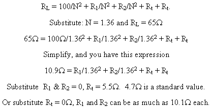
R1 and R2 can be combined into a single component to provide series current limiting to protect the transformer. Resistance on the device side of the transformer must be divided equally in the TIP and RING circuits so that the line is balanced.
3.3 Volt Devices Devices operating from a 3.3 volt supply require a 1: 2 step up transformer to produce a sufficient voltage pulse on the transformer secondary. The same 3 volt pulse over a 100 ohm load is required. In order to produce a 30mA current in the transformer secondary and in the 100 ohm load, a current pulse of 30mA × 2 = 60mA is required from the transmitter output drivers. Adding series resistance to this network would require a turns ratio greater than 1: 2 and thus even larger currents from the transmitter . For this reason it is recommended that 3.3 volt networks be designed with 0Ω of series resistance, and other components be used for over voltage protection. Specifically, Schottky diodes placed in a bridge configuration connected to TTIP and TRING. Schottky diodes turn on sooner than the silicon diodes in the transmit output drivers and so energy is conducted away the CMOS device. See app note 324. 

DS2151 and DS2152-Gener designed for general network interface standards
Figure 1 illustrates a general form of the interface circuit for T1 transceiver chips. Not all of the components are necessary in all applicaTIons. This circuit is used to illustrate how to distribute resistance around the transformers. ApplicaTIon note 324 discusses over voltage protecTIon in more detail .