Power converters for various applications are moving from pure silicon IGBTs to SiC/GaN MOSFETs. Some markets (such as the motor-driven inverter market) are slow to adopt new technologies, while others (such as solar inverters, electric vehicle traction inverters and charger markets) play a key role in innovation. It is expected that the solar market will grow at a compound annual growth rate of 10% for the next five years, and it is very optimistic. The price of photovoltaic systems is expected to drop by another 20%. This is probably the result of technological advances in the photovoltaic inverter electronics. New technologies for power switching (SiC/GaN MOSFETs) will increase the switching frequency, thereby reducing the inductor and capacitor size, while requiring more accurate, faster, and more energy-efficient detection, control, and driver ICs. By 2021, among all the inverters in the power station class, a 1500 VDC power station series string inverter of 30 kW to 100 kW will occupy more than 90% of the market share. They represent benchmarks for new high-density SiC/GaN power switches using innovative multilevel topologies. New disruptive applications such as electric vehicle (EV) and energy storage systems (ESS) have created the need for ultra-high efficiency, high power density, high-frequency SiC power converters. On-vehicle traction motor drives are expected to achieve the highest power density to reduce size and weight, and refresh new efficiency records, while off-board quick chargers are seeking high voltages (up to 2000 VDC, > 150 kW) and complex high frequency topologies. Reduce the overall system cost of magnetic components, mechanical components and assemblies. In addition, these new applications are also driving the development of innovative multi-core control processors, and can manage complex control algorithms to ensure system efficiency and stability in bidirectional mode (from AC grid to DC load and vice versa). . Figure 1. Analog Devices IC Ecosystem Driving SiC/GaN power switches requires the design of a complete IC ecosystem that is precisely tuned and matched to each other. The design focus is no longer just centered on the switch and must be expanded. The application's operating frequency, efficiency requirements, and topology complexity require the use of best-in-class isolated gate drivers (such as the ADuM4135) powered by high-side isolated power circuits (such as the LT3999). Control must be accomplished using a multicore control processor (such as the ADSP-CM419F) that integrates an advanced analog front end and specific security features. Finally, using a power-efficient, isolated ∑-∆ converter (such as the AD7403) to sense the voltage, the design is compact. During the transition from Si IGBTs to SiC MOSFETs, hybrid topology must be considered, where SiC MOSFETs are used for high frequency switching and Si IGBTs are used for low frequency switching. Isolated gate drivers must be able to drive different required switches, many of which are in parallel and use silicon IGBT/SiC MOS hybrid multilevel configurations. Customers want a device to meet all their application requirements, simplifying the BOM and reducing costs. Using a multi-level converter it is easy to reach high operating voltages above 1500 VDC (eg, large-scale energy storage using 2000 VDC), and this type of voltage is a major challenge for isolated barriers implemented for safety. The ADuM4135 isolated gate driver uses ADI's proven iCoupler® technology, which offers many important advantages for high voltage and high switching speed applications. The ADuM4135 is the best choice for driving SiC/GaN MOS, with excellent propagation delays better than 50 ns, channel-to-channel matching less than 5 ns, common-mode transient immunity (CMTI) better than 100 kV/μs, and a single package capable of supporting up to 1500 VDC full-life operating voltage. Figure 2. ADuM4135 Evaluation Board The ADuM4135 is available in a 16-pin, wide-body SOIC package and includes a Miller clamp to enable robust SiC/GaN MOS or IGBT monorail shutdown for gate voltages below 2 V. The output side can be powered by a single or dual power supply. The desaturation detection circuit is integrated on the ADuM4135 to provide high voltage short-circuit switch protection. Desaturation protection includes functions that reduce noise interference, such as providing a 300 ns mask time after switching, to mask voltage spikes that occur at initial turn-on. An internal 500 μA current source helps to reduce the number of devices; for improved noise immunity, internal blanking switches also support the use of external current sources. Taking into account the IGBT general threshold level, the secondary UVLO is set to 11 V. ADI's iCoupler chip-scale transformers also provide isolation of control information between the high and low side of the chip. Chip status information can be read from the dedicated output. The primary control device of the device is reset after the secondary side fails. For more compact pure SiC/GaN applications, the new ADuM4121 isolated gate driver is the solution. The driver is also based on Analog Devices, Inc. iCoupler digital isolation technology with the lowest propagation delay (38 ns) in its class, supporting the highest switching frequency and the highest common-mode transient immunity of 150 kV/μs. The ADuM4121 offers 5 kV rms isolation in a wide body 8-lead SOIC package. Figure 3. ADuM4135 block diagram Figure 4. ADuM4121 Block Diagram Figure 5. ADuM4121 Evaluation Board When an isolated gate driver is used in a high speed topology, it must be properly powered to maintain its performance level. ADI's LT8304/LT8304-1 are single-chip, micropower, isolated flyback converters. These devices directly sample the isolated output voltage from the primary flyback waveform without the need for a third winding or isolator. The output voltage is programmed through two external resistors and a third optional temperature compensation resistor. The boundary mode of operation provides a small solution with excellent load regulation. The low ripple burst mode of operation maintains high efficiency at light loads while minimizing output voltage ripple. The thermally enhanced 8-pin SO package integrates a 2 A, 150 V DMOS power switch and all high voltage circuitry and control logic. The LT8304/LT8304-1 support an input voltage range of 3 V to 100 V, providing up to 24 W of isolated output power. ADI's LT3999 is a single-chip, high-voltage, high-frequency DC-DC transformer driver that provides isolated power and a small solution size. The LT3999's maximum switching frequency of 1 MHz, external synchronization capabilities, and a wide input operating voltage range of 2.7 V to 36 V represent the highest level of technology for providing stable controlled harmonics and isolated power for high speed gate drivers. It is available in exposed paddle 10-lead MSOP and 3 mm × 3 mm DFN packages. Figure 6. LT3999 Evaluation Board System control units (typically combinations of MCUs, DSPs, or FPGAs) must be able to run multiple high-speed control loops in parallel and also manage safety features. They must provide redundancy and a large number of independent PWM signals, ADCs, and I/Os. Analog Devices' ADSPCM419F allows designers to manage parallel high-power, high-density, mixed-switch, multi-level power conversion systems through a mixed-signal dual-core processor. Figure 7. ADSP-CM419F Block Diagram The ADSP-CM419F is based on the ARM® Cortex®-M4 processor core. The floating-point unit operates up to 240 MHz and includes an ARM Cortex-M0 processor core operating at up to 100 MHz. This allows a single chip to integrate dual-core security redundancy. The main ARM Cortex-M4 processor integrates 160 KB of SRAM memory with ECC (Error Checking and Correction), 1 MB of flash memory with ECC, accelerators and peripherals optimized for power converter control (including 24 independent PWMs), And an analog module consisting of two 16-bit SAR ADCs, a 14-bit M0 ADC, and a 12-bit DAC. The ADSP-CM419F is powered from a single supply and uses its internal regulator and an external regulator to generate its own internal voltage source. It is available in a 210-pin BGA package. Figure 8. ADSP-CM419F Evaluation Board Fast and accurate voltage detection is an essential feature of high-speed design. ADI's AD7403 is a high-performance second-order sigma-delta modulator that converts analog input signals into high-speed (up to 20 MHz) single-bit data streams. The 8-pin wide body SOIC package integrates high-speed complementary metal oxide semiconductor (CMOS) technology with single-chip transformer technology (iCoupler technology). The AD7403 operates from a 5 V supply and can accept differential signals of ±250 mV. The original information can be reconstructed with a suitable digital filter to achieve 88 dB signal-to-noise ratio (SNR) at 78.1 kSPS. In order to enable customers' next-generation power converter designs with high performance, high reliability, and market competitiveness, ADI has decided to develop various hardware and software design platforms that can be used to evaluate ICs as building blocks for complete systems. . These design platforms are currently being introduced for strategic customers and represent the highest level of a complete IC ecosystem that drives the new generation of SiC/GaN power converters. There are many types of design platforms, including isolated gate driver boards for high-voltage, high-current SiC power modules, and complete AC/DC bidirectional converters, where the software of the ADSP-CM419F is used to properly control SiC/GaN power switches. The key role.
"Non-burning, nicotine for users, low tar content. As the heating temperature (below 500℃) is lower than the combustion temperature of traditional cigarettes (600-900℃), the harmful components produced by tobacco high-temperature combustion pyrolysis and thermal synthesis are reduced, and the release amount of side-flow smoke and environmental smoke (second-hand smoke) is also greatly reduced."
Heating non - combustion products are electronic devices containing tobacco. When you heat them, they produce a nicotine-containing vapor that you can inhale. Hnb Device Oem,Hnb Device Patent,Hnb Device,Hnb Device For Sale Shenzhen MASON VAP Technology Co., Ltd. , https://www.disposablevapepenfactory.com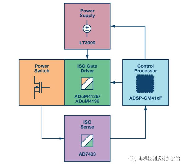


They are different from traditional cigarettes and work by heating tobacco to a very low temperature. Tobacco is heated to 350 ° C in a heat-incombustible device, while traditional cigarettes burn at up to 900 ° C.
Still, the temperature at which non-combustion products are heated is high enough to vaporize and inhale harmful chemicals.
Although both are electronic devices, heated non-combustible products are also different from e-cigarettes or steam devices. These usually use chemical liquids and do not necessarily contain nicotine. E-cigarettes tend to heat liquids to around 250 degrees Celsius to produce vapor.