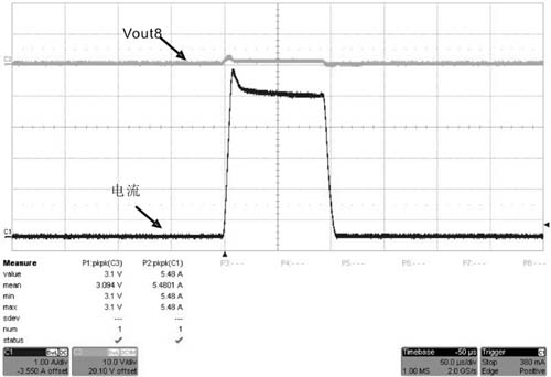
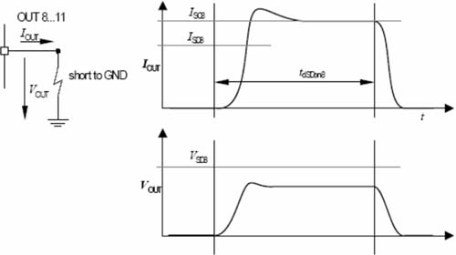
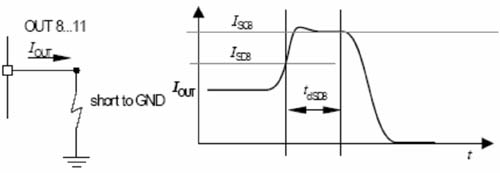
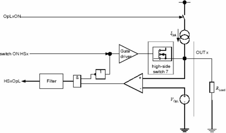
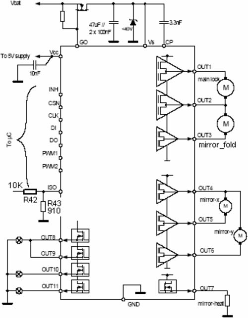
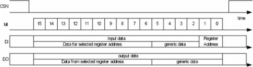
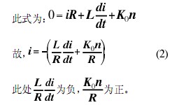
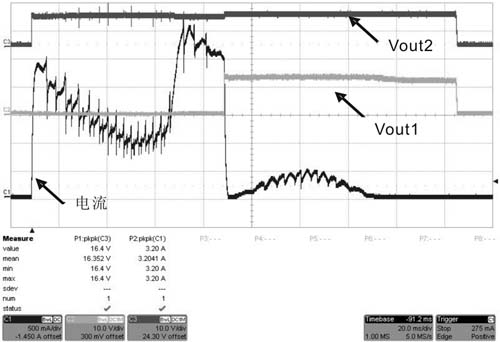
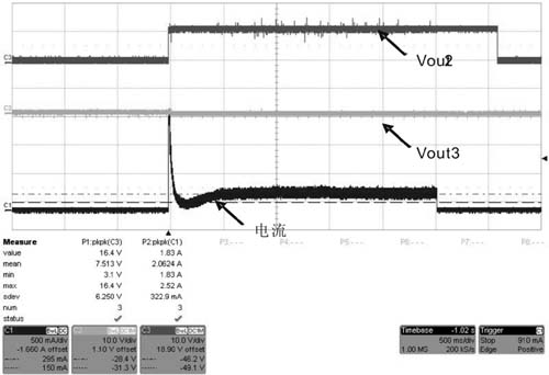
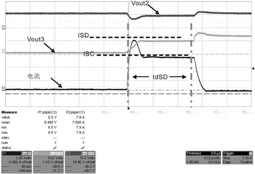
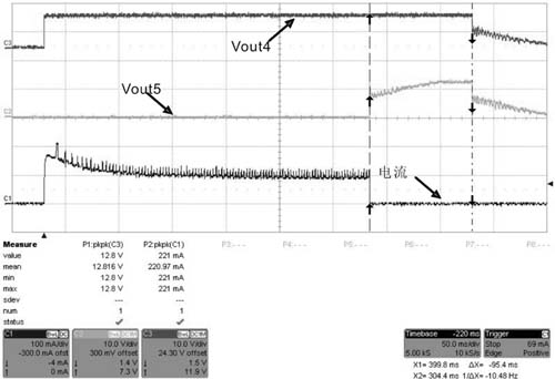
TLE8201 This article refers to the address: http:// The TLE8201 is a highly integrated power ASSP (special standard product) for door modules. These include the power levels necessary to drive loads in typical front door applications, including central locking, deadlock or mirror folding, mirror positioning, mirror heating, and 5W or 10W headlights or LEDs. (such as turn signals, gated room lights / safety warning lights or control panel lights). Figure 1 TLE8201 block diagram The TLE8201 features short-circuit and over-temperature protection and comprehensive diagnostics in accordance with automotive application safety regulations. The current sense output improves the overall performance of the system. The standard SPI interface not only reduces the length of the microcontroller I/O lines, but also provides flexible control of the power stage and provides complete diagnostics. The TLE8201 has two PWM inputs, each of which is a direct power stage control input, which enhances the flexibility of PWM mapping. The information in the SPI register defines the power level that will be controlled by the PWM input. The PWM function can be configured to support up to eight power transistors. The device is available in a Power-SO package with a large thermal block for good thermal resistance. The pins are optimized for efficient PCB design. The application of the TLE8201 not only helps save PCB area and saves costs, but also enhances system quality and increases throughput. TLE8201 application circuit Figure 2 shows the TLE8201 application circuit in the door control module. Figure 2 application circuit power supply The TLE8201 has two power inputs: all power drivers are connected to the supply voltage Vs pin that is connected to the car's 12V power line. The internal logic section is powered by a separate 5V Vcc voltage. In this way, even if a short power outage occurs in Vs, it is ensured that the information stored in the logic circuit is not affected. The TLE8201 requires external reverse polarity protection with a charge pump output for connection to an external n-channel logic level MOSFET. The connection method of the protection circuit is as shown in FIG. 2, and the gate voltage is supplied by the pin GO. The TLE8201 can be placed in low power mode by setting the INH input to "Low". In Sleep mode, all output transistors are turned off and the SPI stops operating. In this mode, the maximum quiescent current is only 6μA (Vs and Vcc). SPI The SPI is used to implement bidirectional communication with the control unit. When the chip is selected by the CSN (chip-select-not) input (H to L) mode, the transmission cycle is started. The 16-bit control word is read through the DI serial data input. The status word is displayed synchronously on the DO serial data output. Synchronous communication is achieved via the serial clock input CLK. As shown in Figure 3, the 16-bit SPI frame consists of an addressable block, an address-independent block, and a 2-bit address, including two control registers and two diagnostic registers. The address independent input section is used for general settings, and the address independent output section is used to mark errors and record temperature information. Figure 3 SPI structure PWM input PWM-ing is a very flexible feature offered by the TLE8201. The required power levels can be controlled in two PWM mode configurations: the PWM1 and PWM2 pins are connected to the microcontroller's timer channel and the desired HSsel bit is selected to activate the PWM function. It is recommended to set the PWM frequency below 200 Hz to minimize power consumption due to switching losses. Current sensing The ISO (inductive output) pin provides a current proportional to the output current flowing to GND at the selected power output. The output is selected via SPI. The induced current is converted to a voltage by an external sense resistor R43 and sent to the A/D converter input. Output stage Outputs 1-6 are half bridges and outputs 7-11 are high side switches. Both the latch motor and the mirror folding motor can be connected to Output 1, Output 2 and Output 3. Output 2 is the sum of the two motor currents. Two rearview mirror positioning motors are connected to output 4, output 5 and output 6. The high side driver output 7 is used to drive the mirror heater. Output 8 and output 9 are used to drive 5W headlights. Output 10 can be coupled to output 11 to collectively drive a 10W headlight. Latch control start up Both output 1 and output 2 of the TLE 8201 are connected to the latch motor. The microcontroller in the door control module communicates with the TLE 8201 via SPI. When the power is turned on, the door lock status is either received by the body control module and transmitted to the door control module, or directly received by the door control module via LIN or CAN. The latch motor is activated when the door or switch panel issues a switch input request or receives a CAN/LIN message from the BCM. Figure 4 shows the startup waveform of the latch motor. Channel 1 is the current flowing through the latch motor. Channels 2 and 3 are the voltage outputs for Output 1 and Output 2 in the TLE 8201. When the PWM soft start is not used, the startup surge current may reach 2A. After startup, the current will drop to around 0.8A. When the latch is completely closed or opened, if the motor stalls, the latch motor can be automatically stopped. When detecting the motor stall, the motor current can be measured through the ISO output of the TLE 8201; the output is connected to the grounding sense resistor R43 and connected to the analog input of the MCU via a protective resistor R42. The block detection criteria are calculated as follows: KILIS12 = 2000, R43 = 910ohm, according to the waveform, the minimum block current is IOUT = 2.5A; then, the block detection voltage can be calculated: Block detection voltage (Vblock-detection) = IISO * R43 = IOUT/KILIS12 * R43 = 2.5A/2000 * 910V/A=1.1375V During the freewheeling process, there is less current, which is the result of the special mechanical structure of the latching motor. There is a spring in the latch to protect the latch from damage, otherwise the latch will slam the top of the door lock. The following is the voltage calculation formula for a common DC motor: Where Vbat represents the external voltage; i represents the motor current; L represents the motor sensor; n represents the motor speed; and R represents the internal motor resistance. When the motor is running at a constant speed, Vbat = iR + K0n (as shown in Figure 1). It should be noted that K0n represents the back electromotive force of the motor. When the motor starts to flow, After the freewheeling, the spring will push the latch motor back slightly because there is no motor current (ie there is no motor torque). That is to say, the speed of the latch motor will change from zero to a negative value, thus generating a positive current through the motor. Figure 4 Latch start waveform Protection and diagnosis In the startup state (ON-state), the load detection can be turned on by the low-side switch of the bridge output: when the current through the low-side transistor is lower than the reference current, and the IOCD is in the startup state for more than the turn-on load detection delay tdOC, The corresponding open load diagnostic bit will be set. However, the output transistors remain activated. The enable load error bit is locked and can be reset by a SPI status register reset or power-on reset. Rear view mirror folding control normal operation The rear view mirror folding motor is driven by the output 2 and output 3 of the TLE8201. Since each half bridge is connected in series and the channel current is also limited, only one motor can be driven at a time. Therefore, as long as the latch motor is running, the mirror output cannot be activated. Figure 5 shows the waveform of the rear view mirror folding motor during normal operation. Channel 1 is the current flowing through the mirror folding motor. Channel 2 is the voltage at output 3 and channel 3 is the voltage at output 2. According to this waveform, the maximum value of the surge current at startup is 2.52A, while the rated current during operation is 0.4A. Figure 5 Waveform of the mirror folding motor during normal operation The electric machine remains running until it locks or exceeds 3 seconds. Because the rear view mirror folding motor uses a special mechanical structure, the load is turned on when the motor is locked! Since the current during the locking process drops to 0A, the motor does not need to be freewheeling. Short circuit protection Figure 6 shows the short circuit protection behavior of the TLE8201. The meaning of each channel is the same as that of FIG. 5. During normal operation, the output 2 (channel 3) voltage is higher and the output 3 (channel 2) voltage is lower. The rated current is 0.4A, which appears to be 0A in Figure 6. When the motor terminal is short-circuited and the current exceeds the output 3 (ISD34 is normally 4A) shutdown threshold ISD for longer than the shutdown delay tdSD, the output transistor of output 3 is turned off and the corresponding diagnostic bit is set. Since the short-circuit shutdown threshold for Output 2 is higher than 8A, the output transistor of Output 2 will continue to operate. Therefore, the voltage of the output 3 is increased to a level equal to the output 2 voltage. During the delay, the current value is limited to the ISC of output 3 (ISC34 is typically 6A). The delay is relatively short (typically 25 microseconds) to reduce energy consumption when the device is shorted. This design provides the peak current required in motor applications. The output stage will remain off and the error bit will be set before the status register reset command is sent to the SPI or a power-on reset is performed. Figure 6 short circuit protection behavior Rearview mirror positioning control Two motors are used, output 4 is connected to the X motor, output 5 is connected to the two motors, and output 6 is connected to the Y motor. Figure 7 shows the waveform of one of the mirror positioning motors in normal operation. When a button is pressed, a certain state is activated. The mirror XY output cannot be activated when the mirror folding motor is active. This type of output does not have PWM control. The surge current at startup is approximately 0.2A and the rated current is 0.1A. Although active braking is not required, the high-side switch remains active for 100 milliseconds of freewheeling time after the mirror has been moved. Figure 7 shows the short circuit protection behavior. The short-circuit protection theory used for outputs 1-6 is identical. The only difference is that the short-circuit shutdown current threshold and the short-circuit current value are different. Figure 7 Waveform of the X-mirror motor during normal operation Figure 8 short circuit protection behavior Rearview mirror defrosting control The PTC heating device is driven by the TLE 8201 output 7. Above a fixed 10 second turn-on time, the output is controlled by a low frequency (eg 10 Hz) PWM with a duty cycle of typically 40%. Control of the PWM is implemented by software via SPI. When the door lock is activated, the heater is turned off to reduce the overall current through the TLE 8201. Headlight control normal operation The gated compartment lights and safety warning lights are driven synchronously by the TLE 8201 outputs 10 and 11. The output is switched on/off by 2 Hz in 200 Hz PWM (theatrical lighting effect). The PWM is controlled by the PWM2 input. The ground protection output short circuit behavior shows the difference between the short circuit that occurs during the turn-on and the short circuit that occurs during the turn-on state. Short circuit during turn-on During the turn-on of the output, the presence or absence of a short circuit is detected by the current and voltage levels. If the switch (if output 8) is turned on and the short-circuit condition is active, the current will exceed the shutdown threshold ISD8 (1.8A to 3.5A) and the output voltage will be lower than VSD8 (1.5V to 3.3V). When tdSDon8 (125 microseconds to 350 microseconds) is exceeded, the output transistor turns off and the corresponding diagnostic bit is set. During the delay, the current value is limited to ISC8 (usually 4.2A), as shown in Figure 9. Channel 1 is the output current and channel 2 is the output voltage. Figure 9 Waveform of short circuit protection during turn-on Figure 10 Short circuit protection during turn-on Short circuit in the open state If the switch is open and a short circuit occurs and the current exceeds the shutdown threshold ISD for more than the shutdown delay tdSD (10 microseconds to 60 microseconds), the output transistor turns off and the corresponding diagnostic bit is set. This mechanism is independent of the voltage Vout. See Figure 11. Figure 11 Short circuit protection in the open state Open load Figure 12 shows the open load of the high side switch in the off state. Turning on load detection is accomplished by comparing the output voltage to the threshold VOpL. The pull-up current can be turned on or off by the OpLxON bit. If an output is used to drive the LED, the OpLxON bit should be set to "Low", which is to cut off the pull-up current, as these LEDs may illuminate in the off state when bias is applied by the pull-up current. Figure 12 Turning on the load in the closed state design Conclusion The TLE8201 is a highly integrated ASSP for door modules. Suitable for driving all loads in typical front door applications, ie central locking, deadlock or mirror folding, mirror positioning, mirror defrosting and 5W or 10W headlights. The TLE8201 offers a variety of protection methods and diagnostics, making it a flexible and reliable device in the door control module. Mini PC
Are you tired on big and messy wires on traditional computer tower? If yes, mini pc bring clean and space saving working environment back to you. Whatever daily tasks, like browsing web pages, documents checking or making, online teaching or learning, entertainments, etc. Or heavy duty handling, like photshops, video or music editing, gaming, apps developing, engineering drawing, designing jobs, etc. You can always find a right pc mini intel at this store.
Mini PC Office is an most and popular series designed for those who mainly run WPS, photoshops, PR, email, entertainments, etc. Sometimes, also call it as mini pc officeworks or home assistant mini pc.
Mini Gaming PC comes with higher level processors, like intel i3, i5, i7 10th, 11th or 12th; bigger memory and storage, like 16GB or 32GB ram, 512gb up to 1tb. Of course, rich slots support linking with two or more monitors or devices.
Except mini pc windows 11, there are also All In One PC , Student Laptop, Gaming Laptop , Android Tablet, Yoga Laptop , etc.
Mini PC Windows 11,High Performance Mini PC,Mini PC DDR4,PC Mini Intel Henan Shuyi Electronics Co., Ltd. , https://www.shuyiaiopc.com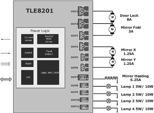
After detecting the block voltage, switch HS1 and HS2 to the "High" position to put the motor into freewheel mode. Both HS1 and HS2 remain high for 100 milliseconds. When switching from L to H, a minimum of 3 microseconds of dead time will occur to ensure that switching slope overlap does not occur, thereby avoiding cross currents. 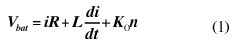
The turn signal (10 w) is driven by the TLE 8201 outputs 8 and 9. The output is controlled by a low frequency (eg 1.5 Hz) PWM with a duty cycle of typically 50%. Control of the PWM is implemented by software via SPI.
Ground protection output short circuit