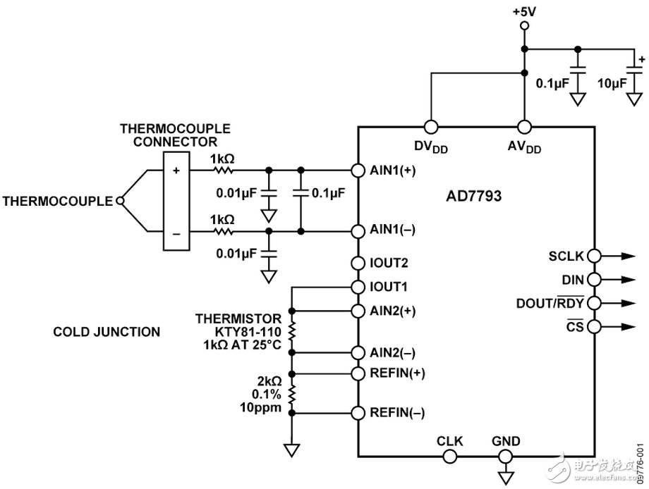
Circuit function and advantage The circuit shown in Figure 1 is a complete thermocouple system based on the AD7793 24-bit Σ-Δ ADC. The AD7793 is a low power, low noise, complete analog front end for high precision measurement applications with built-in PGA, voltage reference, clock and excitation current, which greatly simplifies thermocouple system design. The system peak-to-peak noise is approximately 0.02 °C. With a maximum power consumption of only 500 μA, the AD7793 is suitable for low-power applications such as smart transmitters where the entire transmitter must consume less than 4 mA. The AD7793 also has a shutdown option. In this mode, the entire ADC and its auxiliary functions are turned off, and the maximum power consumption of the device is reduced to 1 μA. The AD7793 provides an integrated thermocouple solution that interfaces directly to a thermocouple. Cold junction compensation is provided by a Thermistor and a precision resistor. The circuit only requires these external components to perform cold junction measurements, as well as some simple RC filters to meet electromagnetic compatibility (EMC) requirements. Figure 1. Thermocouple measurement system with cold junction compensation (schematic diagram: decoupling and all connections not shown) Circuit description This circuit uses a T-type thermocouple. The thermocouple consists of copper and constantan with a temperature measurement range of −200°C to +400°C and produces a temperature-dependent voltage of typically 40 μV/°C. The transfer function of the thermocouple is not linear. In the temperature range of 0 ° C to +60 ° C, the response is very close to linear. However, over a wider temperature range, a linearization procedure must be used. The test circuit does not include a linearization function, so the useful measurement range for this circuit is 0°C to +60°C. Within this temperature range, the thermocouple produces a voltage from 0 mV to 2.4 mV. The internal 1.17 V reference is used for thermocouple conversion. Therefore, the gain configuration of the AD7793 is 128. The AD7793 operates from a single supply and the signal generated by the thermocouple must be biased above ground to be within the range supported by the ADC. For a gain of 128 times, the absolute voltage at the analog input must be in the range of GND + 300 mV to AVDD – 1.1 V. The on-chip bias voltage generator on the AD7793 biases the thermocouple signal to a common-mode voltage of AVDD/2, ensuring that the input voltage limit is met with considerable margin. The thermistor has a value of 1 kΩ at +25°C, a typical value of 815 Ω at 0°C, and a typical value of 1040 Ω at +30°C. Assuming that the transfer function from 0 ° C to 30 ° C is linear, the relationship between the cold junction temperature and the thermistor R is: Cold junction temperature = 30 &TImes; (R – 815) / (1040 – 815) The 1 mA excitation current of the AD7793 is used to power the thermistor and 2 kΩ precision resistors. The reference voltage is generated using this 2 kΩ external precision resistor. This architecture provides a ratiometric configuration in which the excitation current is used to power the thermistor and generate a reference voltage. Therefore, the deviation of the excitation current value does not change the accuracy of the system. When sampling the thermistor channel, the AD7793 operates with 1x gain. For a maximum cold junction temperature of +30 °C, the maximum voltage developed across the thermistor is 1 mA & TImes; 1040 Ω = 1.04 V. The thermistor is selected such that the maximum voltage generated across the thermistor multiplied by the PGA gain is less than or equal to the voltage developed across the precision resistor. For the converted value of ADC_CODE, the corresponding thermistor value R is equal to: R = (ADC_CODE – 0x800000) &TImes; 2000/223 Also consider the output compliance voltage of the AD7793 IOUT1 pin. With a 1 mA excitation current, the output compliance voltage is equal to AVDD – 1.1 V. From the above calculations, the circuit satisfies this requirement because the maximum voltage of IOUT1 is equal to the voltage across the precision resistor plus the voltage across the thermistor, equal to 2 V + 1.04 V = 3.04 V.
Water-cooled capacitor is supercapacitor is a capacitor with a capacity of thousands of farads.According to the principle of capacitor, capacitance depends on the distance between the electrode and electrode surface area, in order to get such a large capacitance, as far as possible to narrow the distance between the super capacitor electrode, electrode surface area increased, therefore, through the theory of electric double layer and porous activated carbon electrode.
Water-Cooled Capacitor,Water-Cooled Power Capacitor,Water-Cooled Electric Heat Capacitor,Water-Cooled Electric Heating Capacitor YANGZHOU POSITIONING TECH CO., LTD. , https://www.cnfudatech.com