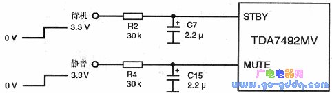
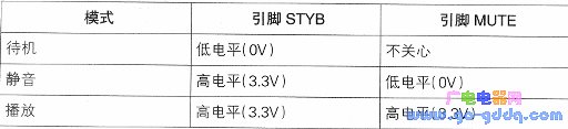
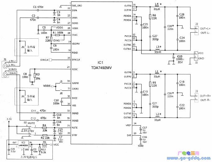
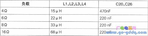
The TDA7492 is a 2x50W stereo bridged load class D audio power amplifier monolithic IC from STMicroelectronics. Its application is mainly for LCD TVs and monitors. Chip circuit composition and pin function The chip circuit TDA7492 is a two-channel BTLD type audio power amplifier integrated circuit. Each channel of the TDA7492 contains an oscillator, a differential input amplifier, level shifting circuitry, high-side (H) and low-side (L) drivers, high/low-side power MOSFETs, protection circuitry, and standby and mute control circuitry. The figure below shows the internal structure of the TDA7492-channel. Package and Pin Function The TDA7492 features a 36-pin bare solder pad in the top PowerSS0-36EPU package, as shown below. The function of each pin is as follows. Main performance and characteristics Single Supply Operation The TDA7492 operates from a wide range of single supply voltages from 8 to 26V with a quiescent supply current of only approximately 26mA. Output power TDA7492, when total harmonic distortion TDH=10%, power supply voltage VCC=25V, when the speaker impedance RL=6Ω, the continuous output power P0=50W+50W, when RL=8Ω, P0=40W+40W. The efficiency amplifier has an efficiency T1 of 90% at an output power of P0 = 2 × 40W. Gain Setting The gain GV of the TDA7492 can be set by the change in the feedback resistance of the amplifier. The TDA7492 has four fixed gains that can be selected via two input pins, GAINO (pin 30) and GAIN1 (pin 31), as shown in the following table. Operating Mode Selection The TDA7492 has three operating modes [Standby, Mute, and Operation (Play)] that can be selected via pins STYB (Pin 20) and MUTE (Pin 21). The standby and mute circuits are shown in the figure below, and the operating mode selection is shown in the table below. Internal and External Clocks The output switching frequency fsw of the TDA7492 can be generated by the internal oscillator. The value is set by the grounding resistor Rosc connected to the IC pin Rosc (pin 24). The calculation formula is fsv=10 to the power of 6/{ [16×Rosc(kΩ)+182kΩ]×4). In the case of the main mode generated by the internal clock, the IC pin SYNCLK (pin 25) is the clock output, and its output frequency is twice the switching frequency of the amplifier. , that is fsyccu (-2 × fsw. To use two or more TDA7492s in the same system, to ensure that each TDA7492 operates on the same frequency, one TDA7492 should be used as the primary clock source and the other TDA7492 as the slave amplifiers. In this case, the output of the primary clock source IC on pin SYNCLK should be connected to the SYNCLK of the slave amplifier, and the SYNCLK of the slave TDA7492 becomes the input. The slave IC's pin ROSC should be left floating, and the slave amplifier output switching frequency fslave is 1/2 of fSYNCLK. Protection Function The TDA7492 provides undervoltage, overvoltage, short circuit and thermal overload protection. Typical Application Circuit The figure above shows a typical application circuit for the TDA7492. In the above figure, the power supply voltage VCC (typically 25V) is added from connector J2, decoupled and bypassed via capacitors C23 and C25, C19, respectively applied to pins ICCA and PVCCB of ICl (TDA7492). VCC also generates a 3.3V voltage through a three-terminal linear buck regulator IC2 as a bias for the standby and mute circuits. With switches S1 and S2, the operating mode of the amplifier can be controlled and selected. If the supply voltage VCC<7V or VCC>28V, the TDA7492's undervoltage protection (U-VP) circuit or overvoltage (OVP) circuit is activated and the amplifier outputs high impedance. Since the IC1 pin Rosc external resistor R3 (Rosc) = 39kQ, the output switching frequency fsw = 310kHz. J8 and J9 are used for single-ended (SE) inputs of two channels, respectively, and J1 is used for differential inputs. The amplifier's common mode noise is minimized when using differential inputs. The input impedance of TDA7492 is 2i=60kΩ, the coupling capacitance Ci (C1, C2 and C11, C12) is 470nF, and the amplifier-3dB cutoff frequency fc=1/(2πRiCi)=5.6Hz. To avoid EMI problems, a low-pass filter is placed between the speaker and the IC1 input. The cutoff frequency of the filter is higher than 22 kHz and much lower than the output switching frequency. The load impedance is different, and the values ​​of the inductor and capacitor components are different, as shown in the following table. The function of the output LC filter is to convert the PWM signal into an analog audio signal. During the operation of the amplifier, if the output current exceeds 6A, or the junction temperature Tj exceeds 1500C, the overcurrent protection (OCP) circuit and the over temperature protection (OTP) circuit are activated to stop the PWM output.
VOZOL BAR 1600 Vape are so convenient, portable, and small volume, you just need to take them
vozol bar 1600 disposable vape,vozol bar 1600 puffs vape,vozol bar 1600 electric cigarette,vozol bar 1600 vape pen,vozol bar 1600 vape kit Ningbo Autrends International Trade Co.,Ltd. , https://www.ecigarettevapepods.com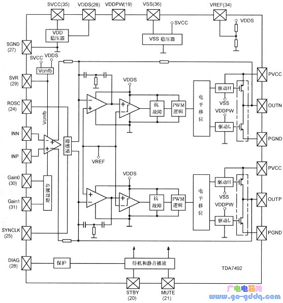
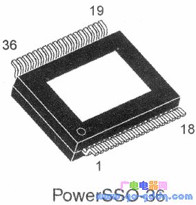
Pin name Features 1 SUB-GND Connected to the frame 2,3 OUTPB Right channel positive PWM output 4,5 PGNDB Right channel power level 6,7 PVCCB Right channel power 8,9 OUTNB Right channel negative PWM output 10,11 OUTNA Right channel negative PWM output 12,13 PVCCA Left channel power 14,15 PGNDA Left channel power level 16,17 OUTPA Left channel positive PWM output 18 PGND Power level 18 VDDPV Power Stage 3.3V Regulator Output 20 STBY Standby mode control input twenty one MUTE Silent mode control input twenty two INPA Left channel positive differential input twenty three INNA Left channel negative differential input twenty four ROSC Main oscillator frequency setting terminal 25 SYNCLK External oscillator clock input/output 26 VDDS Signal circuit 3.3V regulator output 27 SGND Signal ground 28 DIAG Open drain diagnostic output 29 SVR Power supply voltage suppression output 30 GAINO Gain setting input (1) 31 GAIN1 Gain setting input (2) 32 INPB Right channel positive differential input 33 INNB Right channel negative differential input 34 VREF Ground referenced VDDS/2 output 35 SVCC Signal circuit power supply 36 VSS 3.3V regulator output with power supply reference EP Exposed soldering plate, connected to ground 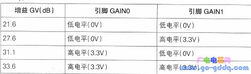
out of your pocket and take a puff, feel the cloud of smoke, and the fragrance of fruit surrounding you. It's so great.
We are China leading manufacturer and supplier of Disposable Vapes puff bars, vozol bar 1600 disposable vape,vozol bar 1600 Puffs Vape,
vozol bar 1600 electric cigarette, and e-cigarette kit, and we specialize in disposable vapes, e-cigarette vape pens, e-cigarette kits, etc.