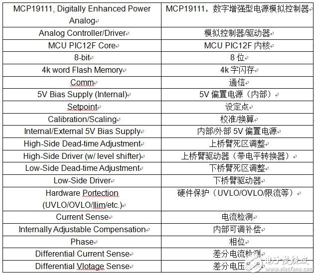
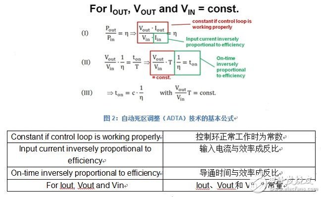
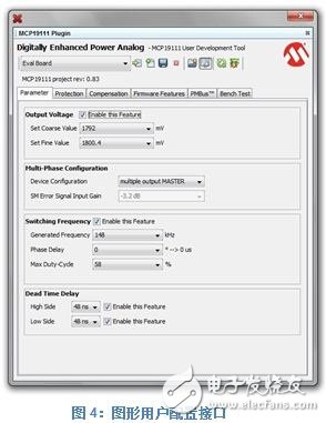
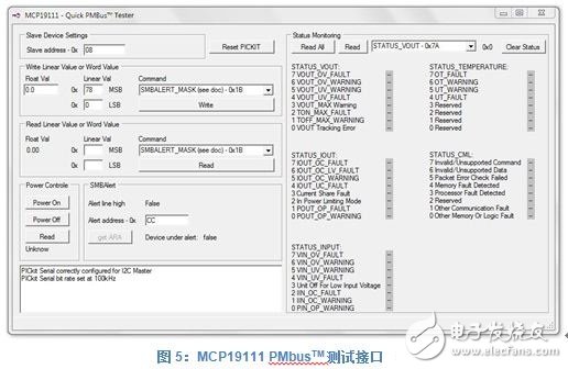
In many systems, a single microcontroller is used to control multiple point-of-load (POL) DC/DC converters to form a hybrid control system to manage system startup behavior, monitor electrical parameters, and manage the power consumption of peripheral subsystems. However, the most complex solution can be found on the CPU blade of a computer motherboard, graphics card or server, where the voltage regulator module (VRM) communicates directly with its load to adjust the supply voltage and/or even adjust its control characteristics to accommodate the temporary Working conditions. This "smart" power conversion management and control has significant advantages in overall system efficiency, performance and reliability - in short: the preferred solution for industrial, medical, automotive and consumer segments. For the last decade, Microchip Technology Inc has focused on so-called intelligent power conversion (IPC/SPC) applications, bringing more features and enhancements to a wide range of power conversion applications. A major focus has been on the use of DSP-based high-performance microcontrollers (high-speed, high-resolution peripherals with high specificity) and dedicated control for hybrid control systems that combine a microcontroller with a full analog control loop. The series is fully digitally controlled for the power converter/inverter. After a more in-depth study of the specific solution, it is clear that the analog-based hybrid control system is not 100% analog, and the all-digital solution is not 100% digital. Both solutions urgently require analog and digital alternatives to overcome specific limitations and have specific advantages for specific target applications. The latest intelligent power conversion controller product line, the MCP191xx, targets dedicated power converter topologies and applications, and it marks a new technological advancement in the intelligentization of power converters. The MCP19111, the first member of the family, combines a high-performance analog synchronous buck converter controller with an 8-bit MCU into a single-chip IC, providing enhanced, flexible configuration, control, and monitoring while allowing the integration of standardized or proprietary communications. To arrange multiple converters in a more advanced power management structure. Unlike other existing hybrid POL controllers, the MCP19111 is fully programmable in C. This advantage provides the flexibility to adjust the device to meet different application requirements, to suit specific operating conditions, and to implement common monitoring tasks and custom functions. The device features a wide DC input voltage range of 4.5V to 32V, an output voltage as low as 0.5V, and a driver that supports up to 2A current/4A sink current, thus supporting a wide range of applications. Digital controllers and analog switching regulators on the same chip allow analog functions to be tightly integrated with digital control, allowing direct manipulation of compensation circuitry, switching frequency, dead-band control, system-level thresholds, and many other functions at runtime. In addition, since the MCU itself is packaged in an analog switching regulator architecture, no additional auxiliary power or external MOSFET drivers are required. Figure 1 shows a high-level block diagram of the MCP19111 digitally enhanced power supply analog controller and a typical application circuit. The analog switching regulator section fully covers all components of the analog control loop (including the MOSFET driver) and also includes the auxiliary power supply for the MCU. The digital portion consists of an 8-bit PIC12F mid-range MCU core, 8 KB of flash memory, and 256-byte RAM. In addition, it provides up to 15 GPIOs (8 of which are additional analog inputs) and 1 based on I? CTM/SMbus serial communication interface, external interrupt and 3 free timers. Many internal signals, such as input voltage, output voltage, or inductor current, can be monitored directly on-chip without external sensing. Digital implementations even allow reading of the current duty cycle, which is still a very useful feature today, but for many technical reasons, it is only available for full digital controllers. In addition to enhanced monitoring capabilities, the digital core's monolithic integrated circuit also allows direct access to many parameters that are typically fixed in hardware or not accessible on silicon. Most notable are adjustable dead zones, programmable compensators, internal feedback calibration, programmable protection thresholds, and the ability to switch between current and voltage mode control during operation. In a synchronous buck converter, the deadband setting between the upper and lower arm switches has a significant impact on overall system efficiency. If the analog controller does not provide any adjustable deadband settings at all, the designer must refer to some worst case scenario that takes into account the highest temperature and load conditions (the deadband usually needs to be set to the maximum value) and "programs" this value. In hardware, for example by placing capacitors and/or resistors. This inevitably increases core and diode losses because the converter is likely to never be placed in these worst case assumptions. A suitable solution is to automatically adjust the deadband to suit specific load and temperature conditions. Unfortunately, there are some serious limitations to using the on-board zero-crossing detector to always drive the switch with the best deadband for two reasons. First, various analog zero-crossing detectors are based on comparators. The fastest (affordable) analog comparator has a typical propagation delay of 15-20 ns. The result is shown in Figure 3. The propagation is too slow to reach the optimal level. Secondly, this zero-crossing detector must operate at the switching node of the half-bridge. There is a high-frequency switching noise that needs to be filtered, which further reduces the triggering speed and eventually causes this function to fail. However, problems that cannot be solved in the analog field will find solutions in the digital field. The most common technique for achieving this optimization is to monitor and analyze the external conditions of the converter until it is stable. As soon as steady state operation is detected, the dead band is modified and the duty cycle of the upper arm switch is monitored. The principle of this constant voltage converter technology is that, under steady state conditions, the shortest relative on-time of the upper arm switch determines the highest efficiency point, because at this point it is only necessary to draw the least power from the bus to provide a certain constant Output power (see Figure 2). Figure 3 shows the results of a single scan over a defined deadband setting during steady state operation, which is measured on the test bench. The green line shows the dead zone (DTR) applied to the rising edge of the upper arm switch. The red curve gives the trend of the on-time of the upper bridge switch under different dead zone settings, and the black dotted line shows its 3rd-order approximation curve. The given dead zone scan range is determined by describing the system characteristics and defining the best case (shortest dead zone) and the worst case (longest dead zone). The scan was performed at a maximum resolution of 4 ns at 90% load (Vin = 12V, Vout = 3.3V, Iout = 9A). On the left side of the figure, the starting value of the duty cycle is about 1.394? s, and as long as the dead zone increases, the duty cycle will decrease rapidly. In this region, the upper and lower arm switches have been shown to overlap, and some of the power drawn from the input is directly shorted to ground. When the dead zone is about 25 ns, the on-time reaches a minimum of 1.384? s, then rises again as the dead zone increases further. In a non-adjustable design, the deadband has been adjusted for at least 70 ns for the switch used, so the typical turn-on time for this operating condition is 1.395? s. According to Equation III in Figure 2, the difference between the original upper arm conduction time and the optimal upper arm conduction time is 11 ns. At first glance, this difference does not seem to be large, but from a high-frequency converter perspective, the difference represents an efficiency gain of about 0.9%, which is equivalent to an increase in total efficiency from about 92% to 93%. Another very good feature is the ability to adjust the compensation network and switching frequency via software. This not only simplifies the basic adjustments during setup configuration, but also allows adjustments to be made at runtime. So far, this is still the core area where all digital controllers have not yet made a breakthrough. In hard-switching topologies such as synchronous buck converters, most of the power is mainly due to switching losses. To increase efficiency (especially under light load conditions), reducing the switching frequency can be a significant aid in improving the overall efficiency of the converter. However, when the switching frequency is reduced, if the compensation network in the hardware is fixed, usually the gain will start to drop and may cause loss of gain margin and phase margin. To compensate for this effect, the gain of the system needs to be adjusted. The MCP19111 provides multiple registers to adjust the PWM generator's ramp voltage, zero frequency (resonant frequency at the origin, defining the first pole), total gain, slope gain, and the slope itself. In addition, there are register banks for adjusting the amplifier offset and current sense gain. While this technique may require lengthy system characterization processes, there is a high probability that efficiency and stability can be significantly improved. In an asynchronous buck converter, the power dissipation in the freewheeling diode is determined by multiplying the forward voltage drop by the current. Since there is a large forward voltage drop across the diode and cannot be minimized, an additional switch with a much lower forward voltage is typically used to bypass/replace the diode, ultimately forming a synchronous rectifier. This technique is often used when the load current exceeds 1A. However, under light load conditions, if very little current flows through the lower arm switch, the power required to drive its gate will exceed the power saved by using the switch bypass freewheeling diode. To further increase efficiency in this particular case, the MCP19111 provides a so-called diode emulation mode that turns off the lower arm driver when this mode is enabled. After the driver is disabled, the gate will no longer be biased and the internal diode of the MOSFET will become the rectifier, minimizing power consumption. Additional support for these measures to minimize partial power consumption and increase overall system efficiency is possible with Microchip's new power MOSFET family, the MCP870xx. This family of fast power MOSFETs features low RDS(on) and balanced quality factor (FOM), which provides a range of different on-resistance and total gate charge (QT) combinations to optimize the total FOM of the half-bridge. The higher the QT of the lower arm switch, the more effective the diode emulation mode of the MCP19111. The MCP19111 is a current mode controller that provides optimum performance during normal operation. However, the current mode controller requires at least some current to flow in order to function properly. When the load is switched to a low-power standby operation, the converter's output must still provide the nominal output voltage, but the output power may be almost zero. Typically, the current mode controller switches to some kind of hick-up mode or pulse frequency mode (PFM) operation with higher output ripple, which exceeds the line regulation tolerance and often causes severe EMI problems. To overcome this limitation of typical current mode controllers, the MCP19111 can be switched to pseudo voltage mode control by disabling the current loop to improve output voltage and system stability. The MCP19111's range of enhancements provide a number of options for configuring and optimizing your system. The open programmability of the MCU adds more freedom. As a result, Microchip provides a graphical user interface (GUI) as shown in Figure 4, allowing users to make specific adjustments and configurations without writing code. This GUI works with open source firmware, which can be modified and used as a template to develop a variety of more advanced features. In addition to configuring the interface, Microchip offers another GUI for testing purposes that allows users to communicate directly with the device via the PMbusTM protocol (see Figure 5). This GUI is used in conjunction with Microchip's PICkitTM Serial Analyzer (part number DV164122), which is a general purpose, low cost USB to UART/SPI/I? C interface, which can be used directly to monitor and debug devices during operation. While most technologies are known and some features can be found in existing devices, the MCP19111 family of devices continues to open a new chapter in the history of smart switching regulators. A number of dedicated features, along with free programmability, highlight its power. In the field of intelligent power controllers, the MCP19111 tightly integrates analog and digital control solutions and enables all functions to be used and accessed by engineers to eliminate existing limitations, thus laying the foundation for innovative, efficient and reliable high performance POL converters The foundation.
Membrane switch is an operating system that integrates key functions, indicating elements and instrument panels. It consists of four parts: panel, upper circuit, isolation layer and lower circuit.
When the membrane switch is pressed, the contacts of the upper circuit are deformed downward, and are in contact with the pole plate of the lower circuit.
After the finger is released, the contacts of the upper circuit bounce back, the circuit is disconnected, and the circuit triggers a signal. The membrane switch has strict structure, beautiful appearance and good sealing performance. It has the characteristics of moisture resistance and long service life.
Widely used in electronic communication, electronic measuring instruments, industrial control, medical equipment, automobile industry, smart toys, household appliances and other fields.
Can provide customers with professional product design. We HAVE accumulated MANY years of experience in Japanese customers, the company has stable quality management experience in mass production orders and can meet the customer's delivery time requirements and quality requirements on time. Now our products are widely used in communications, medical, electronics, digital, watches, automobiles and other high-end fields. With the ISO9001 factory certification, we have gradually become the industry leader with good management, leading technology, excellent quality, timely delivery and thoughtful service. Membrane Switches, Poly Membrane Switches, Home Appliance Membrane Switch, Membrane Switch with Leds China Diy Membrane Switch KEDA MEMBRANE TECHNOLOGY CO., LTD , https://www.kedamembrane.com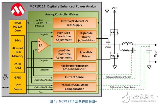
New smart power supply combining analog and digital control
Introduction