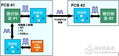
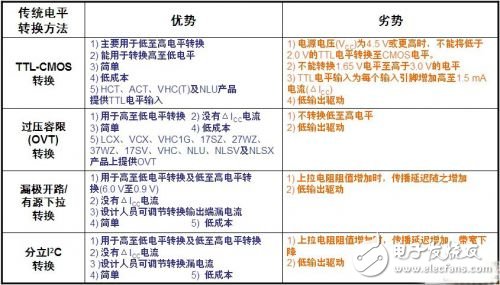
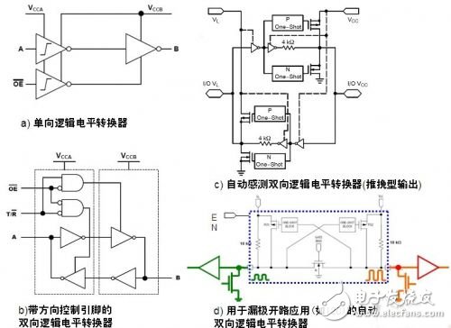
In recent years, driven by Apple's iPhone, the smartphone market has expanded rapidly. An important feature of portable products such as smartphones is the increasing functionality to support a wider range of consumer needs. However, the operating voltages of integrated circuits (ICs) or modules used to support different functions inside portable products such as smart phones are often different. For example, the baseband processor and application processor voltages are generally between 1.5 V and 1.8 V, and many existing ones are available. The operating voltage is generally 2.6 to 3.3 V. For example, the USIM card, Wi-Fi module, and FM tuner module operate at 2.8 V, while the camera module is 2.7 V. Figure 1: Schematic diagram of a logic level shifter application. Therefore, there is an input/output voltage mismatch between different ICs and peripheral modules in portable products such as smart phones. In order for these devices to communicate with each other, efficient logic voltage level conversion is required. The so-called logic level converters are ICs and modules or printed circuit boards (PCBs) that connect different operating voltages to provide a system integration solution. Traditional logic level conversion method and its advantages and disadvantages Table 1: Traditional logic level conversion methods and their advantages and disadvantages. Since transistor-transistor logic (TTL) and complementary metal-oxide-semiconductor (CMOS) are standard levels in logic circuits, TTL-CMOS input conversion is common in traditional logic level shifting methods. This conversion method is simple and low in cost, and is mainly used for low-to-high level conversion, and can also be used to convert high level to low level. This conversion method also has some disadvantages. Other traditional logic level conversion methods include overvoltage tolerance (OVT) voltage conversion, open-drain (OD)/active pull-down conversion, and discrete I2C conversion, each with its own advantages and disadvantages. See Table 1. Dual power logic level conversion and application Power is consumed in logic level shifting. For example, in a low-to-high transition, in order to output a high logic level, the input voltage (Vin) is lower than VCC, and the power supply current variation (ΔICC) is always higher, so the power consumption is also higher. In order to solve the problem of high power consumption, dual supply voltage (VCCA and VCCB) logic level converters can be used. When the logic supply voltage (VL) is equal to Vin, ΔICC is 0, thereby reducing power consumption. Common dual-supply logic level shifting includes unidirectional conversion, bidirectional conversion with directional control pins, auto-sensing bidirectional conversion (push-pull output), and automatic sensing bi-directional conversion for open-drain applications such as I2C The structure diagram is shown in Figure 2. Figure 2: Schematic diagram of several dual-supply logic level shifters. In these dual-supply logic level shifting methods, the principle of unidirectional logic level shifting is to provide A-to-B-point conversion when Output Enable is low, and when the output is enabled high. A high-impedance state (Hi-Z) is present between A and B, which is usually treated as a resistor infinity, which is equivalent to no connection. Common dual-supply unidirectional logic level shifters are such as ON Semiconductor's NLSV1T34AMX1TCG, NLSV2T244MUTAG, NLSV4T3234FCT1G, NLSV8T244MUTAG, NLSV22T244MUTAG, and so on. Applications for these dual-supply unidirectional logic level shifters include general purpose input and output (GPIO) ports, serial peripheral interface (SPI) ports, and universal serial bus (USB) ports. The bidirectional logic level shifter with directional control pin works by providing a B-to-A conversion when the pin and direction control (DIRecTIon, T/) pins are low; the pin is low When the T/ pin is high, the A point to the B point conversion are provided; and when the pin is high level, the A point to the B point direction and the B point to the A point direction are in a high impedance state, which is equivalent to no connection. through. ON Semiconductor is about to introduce a bidirectional logic level shifter with directional control pins. A common application for such converters is memory and I/O devices that are accessed in bytes. The automatic sensing bidirectional logic level shifter (push-pull output) works by setting the enable (EN) pin low when the converter is in standby; the EN pin is high, I/O level When the constant is unchanged, the converter is in steady state; when the EN pin is high and the I/O level changes, the converter detects the change and generates a pulse, and the I/O is pulled up by the P-channel MOSFET (PMOS) to Faster. Typical auto-sensing direction bidirectional logic level shifters (push-pull outputs) are such as ON Semiconductor's NLSX3012MUTAG, NLSX3013FCT1G, NLSX3013BFCT1G, NLSX4014MUTAG, and NLSX3018MUTAG. Common applications for such converters include Universal Asynchronous Receiver Transmitter (UART), USB ports, 4-wire SPI ports, and 3-wire SPI ports. The auto-sensing bidirectional logic level shifter for open-drain applications (such as I2C) also contains three states: the EN pin is high, the NMOS is on, it is active, and the input I/O level Pull down to ground, that is, input low level; EN pin is high level, NMOS is in high impedance state, it is in working state, output I/O level is pulled up to VCC, ie input high level; EN pin When low, the converter is in standby. Typical automatic sensing bidirectional logic level shifters for open-drain applications such as I2C are such as ON Semiconductor's NLSX4373MUTAG, NLSX4348FCT1G, and NSLX4378BFCT1G. Common applications for such converters include the I2C bus, Subscriber Identity Module (SIM) card, single-wire (1-Wire) bus, display module, Secure Digital Input Output (SDIO) card, and more. Among the above-mentioned dual-supply logic level shifters, the automatic sensing converter without the direction control pin and the converter with the direction control pin have their advantages and disadvantages. The advantages of the auto-sensing converter are mainly to minimize the I/O line of the microcontroller. It is a simple solution for asynchronous communication. The disadvantage is that the cost is higher than the converter with lower bandwidth than the control pin with direction. . The converter with directional control pins has the advantage of being a commodity component with low cost and is a simple solution for memory-mapped I/O. The disadvantage is the large number of microcontroller pins. In automatic sensing converters without directional control pins, there are also differences between integrated solutions (such as NLSX3373) and discrete solutions (such as NTZD3154N). The integrated solution NLSX3373 is a single IC, which is estimated to occupy only 2.6 mm2 of printed circuit board (PCB) space. The discrete solution NTZD3154N uses dual MOSFETs and four 01005 packages (ie 0402) resistors. The estimated total PCB space is 3.3. Mm2. The integrated solution provides a low-power standby mode, while the discrete solution does not provide a high-impedance/standby mode. The low voltage operating characteristics, bandwidth and circuit characteristics of the two different solutions are also different. Fiber Optic Splice Closure,Fiber Optic Splice Case,Fiber Splice Closures,Outdoor Fiber Optic Splice Closure Cixi Dani Plastic Products Co.,Ltd , https://www.danifiberoptic.com