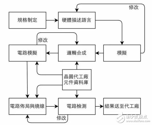
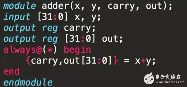
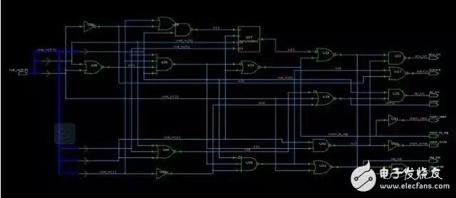
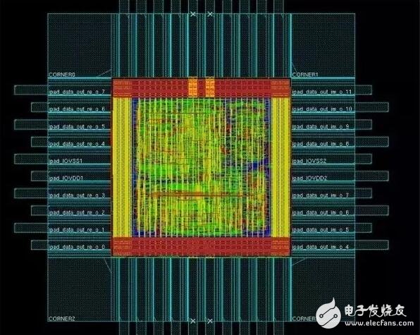
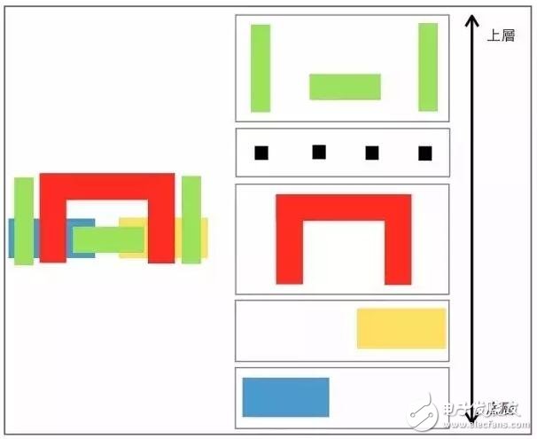
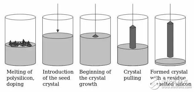
Complex and cumbersome chip design process The process of chip manufacturing is like using LEGO to build a house. First, the wafer is used as the foundation. After the layer is stacked on the chip manufacturing process, the necessary IC chips can be produced (these will be described later). However, without a design, it is useless to have a strong manufacturing capability, so the role of the architect is very important. But who is the architect in IC design? This article will next introduce the IC design. In the IC production process, ICs are mostly planned and designed by professional IC design companies. For example, MediaTek, Qualcomm, Intel and other well-known manufacturers have designed their own IC chips to provide chips of different specifications and performances for downstream manufacturers. Because ICs are designed by each factory, IC design relies heavily on the engineer's technology, and the quality of the engineer affects the value of an enterprise. However, what steps do engineers have when designing an IC chip? The design process can be simply divided into the following. Design first step, set goals In IC design, the most important step is specification development. This step is like deciding to have several rooms and bathrooms before designing the building. What building regulations are required to follow, and designing after all the functions have been determined, so that no additional time is required for subsequent modifications. IC design also requires similar steps to ensure that the designed chip does not make any mistakes. The first step in the specification development is to determine the purpose and performance of the IC and to set the direction. Then it is to see which agreements are to be met. Chips like wireless network cards need to comply with IEEE 802.11. Otherwise, the chip will not be compatible with the products on the market, making it impossible to connect with other devices. Finally, the implementation method of this IC is established, the different functions are assigned to different units, and the method of connecting different units is established, so that the specification is completed. After designing the specifications, the details of the design chip are followed. This step is like taking a preliminary record of the building's plan and drawing out the overall outline to facilitate subsequent drawing. In the IC chip, the circuit is described using a hardware description language (HDL). The commonly used HDL has Verilog, VHDL, etc., and the function of an IC can be easily expressed by the code. The next step is to check the correctness of the program's functionality and continue to modify it until it meets the desired functionality. ▲ Verilog example of the 32 bits adder. With the computer, things are easy With the full plan, the next step is to draw a flat design blueprint. In IC design, the logical synthesis step is to put the unambiguous HDL code into the electronic design automation tool (EDA tool), and let the computer convert the HDL code into a logic circuit to produce the following circuit diagram. After that, it is repeatedly determined whether the logic gate design conforms to the specifications and is modified until the function is correct. ▲The result of the synthesis of the control unit. Finally, the synthesized code is placed in another EDA tool for Place And Route . After continuous testing, the following circuit diagram will be formed. Different colors such as blue, red, green, and yellow can be seen in the figure, and each different color represents a mask. As for how to use the mask? ▲ Commonly used calculus chip - FFT chip, complete the circuit layout and winding results. Layered reticle, stacking a chip First of all, it is known that an IC will produce multiple masks. These masks have separate layers, each with its own task. The following figure shows a simple reticle example. Take the most basic component CMOS in the integrated circuit as an example. The CMOS is called Complementary Metal-oxide-semiconductor, which means that both NMOS and PMOS are used. Combined to form a CMOS. As for what is a metal oxide semiconductor (MOS)? Such components that are widely used in chips are difficult to explain, and it is difficult for general readers to clarify them. In the figure below, the left side is the circuit diagram formed after the circuit layout and winding. It is known in the front that each color represents a mask. On the right is the way to spread out each mask. The production is started from the bottom layer, following the method mentioned in the previous IC chip manufacturing, layer by layer, and finally the desired chip will be produced. To this, for IC design should have a preliminary understanding, it seems very clear that the overall IC design is a very complex profession, thanks to a computer-aided software maturity, so that IC design is accelerated. The IC design factory relies heavily on the wisdom of engineers. Each step described here has its own specific knowledge. It can be independently developed into a number of professional courses. For example, writing a hardware description language is not a simple matter. You also need to understand how logic circuits work, how to convert the required algorithms into programs, and how synthetic software converts programs into logic gates. Among the major semiconductor design companies are Intel, Qualcomm, Broadcom, NVIDIA, Dimensions, Xilinx, Altera, MediaTek, HiSilicon, Spreadtrum, ZTE Microelectronics, Huada, Datang, Zhixin, Duntai, Silan, Zhongxing , Geke and so on. What is a wafer? In the semiconductor news, there are always mentions of size-named fabs, such as 8-inch or 12-inch fabs. However, what is the so-called wafer? Eight-inch section refers to what? What is the difficulty in producing large-size wafers? The following is a step-by-step introduction to the most important foundation of semiconductors - what is "wafer"? Wafer (wafer), is the basis for manufacturing various types of computer chips. We can compare the chip manufacturing to the house with Lego bricks, and complete the desired shape (that is, various chips) by stacking one layer after another. However, if there is no good foundation, the house that is covered will come and go, not what you want. In order to make a perfect house, you need a smooth substrate. For chip manufacturing, this substrate is the wafer that will be described next. (Souse: Flickr/Jonathan Stewart CC BY 2.0) First of all, let's first think about the fact that when you are a child, you will have a small round protrusion on the surface of the building block. With this structure, we can firmly stack the two blocks without using glue. . Chip fabrication, in a similar manner, holds the subsequently added atoms and substrate together. Therefore, we need to find a substrate with a neat surface to meet the conditions required for subsequent manufacturing. In a solid material, there is a special crystal structure of single crystal ── (Monocrystalline). It has the characteristics that atoms are arranged one after another and can form a flat atomic surface. Therefore, using a single crystal to form a wafer can meet the above requirements. However, how to produce such a material has two main steps, namely purification and crystal pulling, and then the material can be completed. How to make a single crystal wafer The purification is divided into two stages. The first step is metallurgical purification. This process is mainly to add carbon to convert the silicon oxide into silicon of 98% or more purity by redox. Most metals are refined, such as metals such as iron or copper, in such a way that metals of sufficient purity are obtained. However, 98% is still insufficient for chip manufacturing and still needs further improvement. Therefore, the Siemens process will be further used for purification, and thus, high-purity polycrystalline silicon required for the semiconductor process will be obtained. ▲ Silicon column manufacturing process (Source: Wikipedia) Then, it is the step of pulling crystals. First, the high-purity polycrystalline silicon obtained above is melted to form liquid silicon. Thereafter, the single crystal silicon seed is brought into contact with the surface of the liquid, and is slowly pulled up while rotating. As for why a single crystal silicon is needed, it is because the arrangement of silicon atoms is the same as that of people, and it will be necessary to arrange the heads so that later people can arrange them correctly. The silicon species is an important leader, so that later atoms know how to line up. Finally, after the silicon atoms leaving the liquid surface are solidified, the aligned single crystal silicon columns are completed. ▲ Monocrystalline silicon column (Souse: Wikipedia) However, what does 8 inch and 12 inch represent? He refers to the crystal column we produced, which looks like the part of the pencil holder, and the surface is treated and cut into thin discs. What is the difficulty in manufacturing large-size wafers? As mentioned above, the production process of the crystal column is like making cotton candy, and it is formed while rotating. If you have made marshmallows, you should know that it is quite difficult to make large and solid marshmallows, and the process of pulling crystals is the same. The speed of rotation and the control of temperature will affect the quality of the crystal column. Therefore, the larger the size, the higher the speed and temperature requirements of the crystal pull, so it is more difficult to make a high-quality 12-inch wafer than the 8-inch wafer. However, a whole silicon column cannot be made into a substrate made of a chip. In order to produce a piece of silicon wafer, the silicon crystal column is then cut into a wafer by a diamond knife, and the wafer can be formed into a wafer by polishing. Fabricate the required silicon wafers. After so many steps, the manufacture of the chip substrate is completed, and the next step is the step of stacking the house, that is, chip manufacturing. As for how to make chips? This Automation curtain is specially designed for automation industry. SDKELI LSC2 light curtain is designed for automation field, with small size, compact structure and strong anti-interference ability, and the product meets IEC 61496-2 standards. The automatic light curtain is with reliable quality and very competitive price. It has been used in many factories and has replaced curtains from Sick, Omron, Banner, Keyence, etc. Automatic Light Curtain,Laser Light Curtain,Automation Light Beam Sensor,Automatic Infrared Beam Sensor,Infrared Beam Curttain Sensor,Infrared Beam Sensor Jining KeLi Photoelectronic Industrial Co.,Ltd , https://www.sdkelien.com