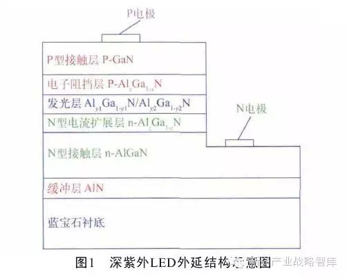
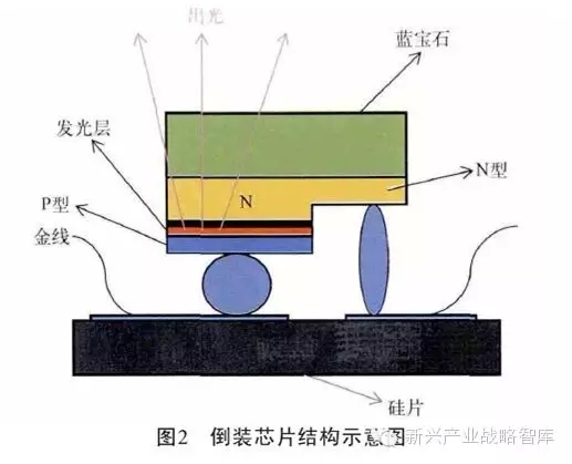
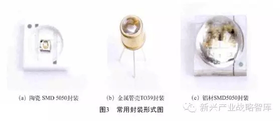
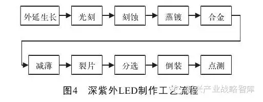
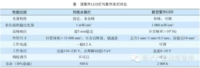
With the continuous development of LED technology, its light-emitting wavelength has been extended from the visible light band to the deep ultraviolet band. The maturity of its technology and the cost reduction will make the UV LED application more extensive and may even surpass the current blue LED. From the aspects of the light-emitting characteristics and manufacturing process of deep-UV LEDs, the current research progress and industrial application of deep-UV LEDs are highlighted. In 1997, Nichia Chemical successfully developed the world's first GaN-based UV-emitting LED with a wavelength of 371 nm. In 2003, SETi Corporation of the United States developed an A1GaN-based deep ultraviolet LED with a wavelength of 280 nm. On October 24, 2014, one of the Nobel Prize winners in physics, Amano, introduced his ongoing research at a press conference, including deep-UV LEDs with wavelengths around 250-350 nm. As a branch of LED, UV LED can not be illuminated but has all the advantages of LED. In theory, it can replace all traditional ultraviolet light sources, greatly expanding the application field of LED. The most common ultraviolet rays are mainly derived from solar radiation. According to the wavelength, ultraviolet rays can be classified into ultraviolet A (UVA), ultraviolet B (UVB) and ultraviolet C (UVC). The wavelengths are 320~. 400 nm, 280~320 nm, 100~280 nm. The ultraviolet rays that can reach the surface of the earth mainly include long-wave ultraviolet UVA and medium-wave ultraviolet UVB, while short-wave ultraviolet UVC is basically absorbed by the ozone layer in the atmosphere (so UVC belongs to the day blind zone). Introduction to UV LED Manufacturing Technology 1.1 Preparation of luminescent materials The epitaxial growth process is to sequentially grow an A1N template layer, an N-type A1GaN layer, a plurality of well light-emitting layers, an electric barrier layer, and a P-type GaN contact layer on a sapphire substrate by an MOCVD apparatus. The epitaxial structure is shown in FIG. 1 below. 1.2 Electrode manufacturing process The chip process, through the lithography, etching leakage N-type contact layer, through evaporation and alloy, N-type, P-type and the electrode form an ohmic contact (Figure 1), and then through the thinning, splitting, small core particles Select and flip it onto the insulated silicon wafer. 2 is a schematic structural view of a flip chip. 1.3 Packaging method The packaging method affects the light extraction efficiency, while the lens package and the non-lens package have a particularly large effect on the light output of the ultraviolet LED. In addition, different heat dissipation and anti-static capabilities caused by different headers will also affect the life of the device. Figure 3 shows the common package form. 1.4 Manufacturing Process The process of deep ultraviolet LED is basically the same as that of blue light. The main difference is that blue light can pass through the top P type, while deep ultraviolet LED can only be flipped out from the back side due to the absorption of p-GaN. The process flow of the deep ultraviolet LED is shown in Figure 4. Current research progress and problems After more than 10 years of research and development, the external quantum efficiency of deep ultraviolet LEDs below 280 nm has exceeded 5%, corresponding to luminous power greater than 5 mW, and lifespan of 5,000 h. The increase in power is driving the development of applications. The applications of deep ultraviolet LEDs include: optical sensors and instruments (230~400 nm), UV identification, bar code (230~280 nm), drinking water sterilization, portable sterilization (240~280 nm) ). 2.1 Low power The external quantum efficiency of deep ultraviolet LEDs has exceeded 5%, but is still very low compared to 60% of blue light for the following reasons. (1) The defect of the template material quality, the dislocation density of the A1N material epitaxially grown on the sapphire is as high as 1×109 cm 2 , and the dislocation density of the GaN material grown on the pattern substrate is about 1×10 7 cm 2 , so the pattern substrate is used to improve the quality of the template material. (2) The total internal reflection loss of deep ultraviolet light in the multilayer structure, and the absorption of the P-type electrode result in poor light extraction efficiency, and the current light extraction efficiency is only 6%. A breakthrough in p-type ohmic contact is required to reduce dependence on highly absorptive p-GaN; to optimize the refractive index difference of the multilayer heterojunction; to use a patterned substrate; to rough out the smooth surface. (3) A1GaN with high aluminum composition will have a significant amount of polarization effect, causing a polarized electric field in the quantum well and the barrier, resulting in an increase in operating voltage and a decrease in quantum efficiency. The solution is to use a non-polar surface (such as a-plane) sapphire as the substrate, or offset by a component grading method. 2.2 poor heat dissipation The low external quantum efficiency causes most of the electrical energy to be converted into thermal energy, so the heat dissipation problem is critical. In terms of chip and package, thin-film inverted deep-UV LEDs and flip-chip deep-UV LEDs can improve heat dissipation and produce high-power deep-UV LEDs. 2.3 Low life Compared with the 100000h of blue light, the life of deep ultraviolet LED is only 5000h, and its low life is mainly attributed to material defects and poor heat dissipation, and the packaging material is susceptible to aging due to ultraviolet radiation. Deep UV LED application The performance comparison between deep ultraviolet LED and traditional ultraviolet mercury lamp is shown in the following table. The advantages of UV LED are as follows. (1) Efficient: The light intensity per unit area exceeds 1,000 times that of mercury lamps. For example, a single LED has a light-emitting area of ​​only 0.3 mm X 0.3 mm but an optical power of more than 1 mW, while a mercury lamp emits less than 1 mW of light on such a small area. (2) Environmental protection: Semiconductor materials are non-toxic and harmless, and UV LEDs do not contain any toxic substances. (3) Energy saving: The same light output power, energy consumption is only 1/10 of the mercury lamp. (4) Reliable: It is reflected in the intelligent control of the switching characteristics and service life. Due to the LED's illuminating characteristics, the pulsed switch has no effect on the life of the LED. When the 6V DC is turned on, the ultraviolet light is emitted simultaneously, and the switch of the mercury lamp directly affects its life, so compared with the conventional mercury lamp, the LED Ultraviolet emission and control is extremely simple and convenient. 3.1 sterilization The UV disinfection wavelength range is 240~300 nm, which can destroy the bacterial replication gene chain and make it impossible to replicate, thus achieving the purpose of sterilization. The sterilization characteristics are as follows. (1) The sterilization process is a physical destruction process. Unlike chemical agents, it is not affected by chemical equilibrium conditions such as temperature, concentration, and activity. (2) Non-toxic, no residue and no odor. (3) Both the cell wall and the viral protein shell are unable to block the deep ultraviolet rays. (4) Uniform destruction of DNA and RNA, without having to replace drugs. (5) It is not necessary to use a combination agent. (6) It is especially suitable for disinfecting the surface of air, water and objects. 3.2 Other application areas of UV LED UV LEDs are used in a wide range of applications and can be used in the following areas. (1) Water purification, killing bacteria and viruses in water, can be used for drinking water purification, household aquarium purification, sewage degradation (dioxin Dioxin), fresh water and marine aquaculture. (2) Air purification, killing bacteria in the air, can be used for air conditioners and humidifiers, UV photocatalyst purifiers, chemical and biomedical air purification. (3) National defense and security, ultraviolet detection, ultraviolet communication, etc. (4) Food processing and preservation, food, beverage and vegetable packaging, meat processing, catering, food retail and refrigerator storage. (5) Medical field, treatment of skin diseases, and cutting off infection routes, public places, school portable sterilization products, etc. The main application market that has been developed recently 4.1 Preparation of luminescent materials Utilizing the penetration of deep ultraviolet rays in water, it effectively kills bacteria and viruses and ensures safe drinking water. Applicable products: household water dispensers, disinfection cups, fish tank sterilization, disinfection pens and other disinfection drinking utensils. 4.2 Air sterilization The use of deep ultraviolet bactericidal function can effectively block the spread of bacteria and viruses in the air. Applicable products: air conditioner (home air conditioner, large air conditioner), humidifier, dehumidifier, air sterilizer (desktop, car). 4.3 Food sterilization The use of deep ultraviolet light to directly illuminate the food attached to the plastic wrap can effectively kill bacteria, molds and even viruses, and prolong the shelf life of the food. Applicable products: refrigerator, various disinfection cabinets, dehumidifiers, air sterilizers (desktop, car). 4.4 Medical equipment It can be used in the two fields of blood therapy and light therapy by utilizing the functions of deep ultraviolet ray sterilization, anti-inflammatory, analgesic, and stimulating antibody growth to accelerate healing. With the increase of the luminous power of UV LEDs and the cost reduction, the future application of UV LEDs will be more extensive, more prominent than the current blue LEDs, and will become one of the most influential semiconductor products of this century. Hengstar designs and develops various industrial LCD displays for industrial control systems. There are multiple installation methods including: desktop installation, universal VESA mount, panel mount, flush mount and rack mount, making our monitors suitable for different types of industrial control and factory automation. industrial displays,industrial monitor,industrial monitors touch screen,Industrial Lcd Monitor,industrial monitoring,large industrial monitors Shenzhen Hengstar Technology Co., Ltd. , https://www.angeltondal.com