IPC is a multi-function touch tablet computer solution that supports Intel Atom D2550 1.86GHz dual-core CPU and DDR memory, equipped with LCD display and five-wire resistive touch screen. The whole machine uses 9 ~ 36V wide voltage DC power supply, front panel IP65 protection built-in power supply optional, equipped with a variety of I / O interfaces and also reserved a 32-bit PCI slot, rack-mounted design, making it the first choice for industrial automation man-machine interface, suitable for factory automation, machinery Host computer control and monitoring of manufacturing, CNC equipment, textile machinery, boiler control, intelligent power equipment, etc. Rack Mount Screen,Rack Mount Monitor,Rack Mount Touch Screen,Rack Mount Computer Monitor Shenzhen Hengstar Technology Co., Ltd. , https://www.angeltondal.com
Introduction With the rapid development of the Internet and the increase in the demand for various wireless services, the current wireless communication network that mainly carries a single voice service has become increasingly unsuitable for people's needs. Therefore, large capacity, high data rate and multimedia The business-oriented third-generation mobile communication system (IMT-2000) has become the development direction of wireless communication. Code division multiple access (CDMA) technology has become the most important multiple access technology in the third generation of mobile communication due to its good noise resistance, confidentiality and low power.
Compared with the traditional CDMA system, the biggest feature of the third generation mobile communication is that it can support multiple speed services, from voice to packet data to multimedia services, and can provide the necessary bandwidth according to the specific business needs. The 3GPP agreement specifies that the service types supported by the WCDMA system include: 5.15Kbps ~ 12.2Kbps voice data, 64Kbps circuit data, 144Kbps packet data and 384Kbps packet data. However, for baseband processing of services of different rates, the required storage, calculation, and processing delays vary greatly. Therefore, what kind of hardware structure can effectively deal with various business is the problem to be discussed in this article.
This article first introduces the baseband transmission scheme of the wireless channel of the WCDMA system, explains its support for multimedia services and the complexity of implementation. Then, from the perspective of hardware implementation, the performance of DSP and FPGA is compared, and the implementation scheme of DSP + FPGA baseband transmission is proposed. Taking the transmission unit of the base station subsystem (BTS) as an example, the implementation scheme is specifically given in the downlink wireless Application in the channel baseband transmission unit.
WCDMA baseband transmission scheme
The transmission unit of the WCDMA system implements baseband data processing of the wireless channel (CRC check, error correction coding, rate adaptation, interleaving, multiplexing, framing), spread spectrum scrambling, combining and power control, shaping filtering, D / A conversion, and finally provided to the analog front end. The following link is used as an example to give the baseband data processing scheme and spread spectrum scrambling modulation scheme.
In the baseband processing flow (as shown in Figure 1), each transport channel (TrCH) corresponds to a service. Due to the different delay requirements of various services, the transmission time interval (TTI) is different (TTI∈ { 10ms, 20ms, 40ms, 80ms}). Specific steps are as follows:
First, the input data within a transmission time interval (TTI) of each transmission channel is divided into transmission blocks, and CRC check bits are added at the end of each block, so that the receiving end can perform error detection.
Secondly, all the transmission blocks added with the check digit are concatenated in series. If the amount of data after concatenation is greater than the specified maximum coding block size, then the concatenated data block needs to be segmented and divided into several coding blocks of the same size, so that the size of each coding block is less than or equal to the maximum coding block size. For different encoding methods, the maximum encoding block size is different. Among them, convolutional coding: Z = 504; Turbo coding: Z = 5114 (Z represents the maximum coding block size).
There are two types of error correction codes used in WCDMA: Turbo codes and convolutional codes. The wireless channel coding is for the receiver to detect and correct the signal error caused by the transmission medium, and at the same time add redundant information to the original data stream to improve the data transmission rate. Compared with Turbo coding, the former has the advantages of fast decoding speed and small delay; but for the higher rate channel, the latter has lower signal-to-noise ratio requirements under the same QoS conditions. For services with small data volume and high real-time requirements, convolutional coding is used, such as voice services; and for services with large data volume and low real-time requirements, Turbo coding is used, such as IP services and multimedia services.
In order to adapt the data of the transmission channel to the physical channel, it is necessary to perform rate adaptation on the encoded data stream. Rate adaptation is to repeat or gouge the data on the transmission channel bit by bit, so that even if the number of data bits on different transmission intervals is different, the total number of data bits after multiplexing of the transmission channel is always constant for a given physical channel .
There are two interleaving operations during the baseband processing of the data block, namely the first interleaving and the second interleaving. The function of interleaving is to scramble the original data sequence, so that the correlation of the data sequence before and after interleaving is weakened, and the system's anti-interference ability against sudden errors is improved. Both interleaving modes use inter-column interleaving mode, that is, data is written into the rectangular array row by row, and then read out column by column according to a certain column interleaving mode.
A transmission channel corresponds to a service type. At the physical layer, sometimes different service data needs to be multiplexed together and transmitted through a physical channel. This process is the multiplexing of services at the physical layer.
The spreading of the physical channel consists of two steps. The first step is channelization, which converts each data symbol into multiple chips to increase the bandwidth of the signal. The number of chips in each data symbol is called the spreading factor (SF); the second step is scrambling, thereby scrambling the spread spectrum signal. In the downlink, the symbol pair composed of two consecutive symbols undergoes serial-to-parallel conversion and is mapped onto the I and Q branches. The result of the mapping is that even-numbered and odd-numbered symbols are mapped onto the I and Q branches, respectively. The I and Q branches are spread to the chip rate with the same real-value channelization codes Cch, SF, and m, and then the real-valued chip sequences on the I and Q branches are converted into complex-valued chip sequences. The sequence is scrambled by complex-valued scrambling codes Sdl, n (multiplication of complex numbers). The specific spread spectrum scrambling block diagram (shown in Figure 2).
The chip rate of the modulated signal is 3.84 Mcps, and the modulation of the complex-valued chip sequence generated by the spreading process is QPSK. The specific modulation block diagram (shown in Figure 3). 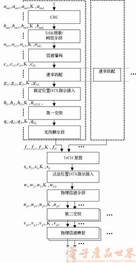
Figure 1 Downlink transmission channel multiplexing structure 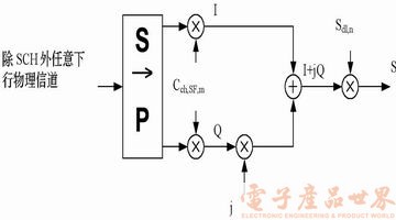
Figure 2 Spread spectrum of all downlink physical channels except SCH 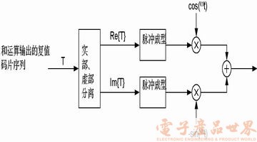
Figure 3 Downlink modulation
The circuit structure of the implementation scheme baseband data processing This paper presents the implementation scheme of "DSP + FPGA linear pipeline array structure": using DSP and large-scale FPGA to co-process baseband transmission data. The processing unit takes the DPS chip as the core and constructs a small DSP system. The circuit structure is shown in Figure 4.
In the baseband processing unit, the low-level signal preprocessing algorithm processes a large amount of data and requires high processing speed, but the operation structure is relatively simple, so it is suitable for hardware implementation with FPGA, which can take into account both speed and flexibility. In contrast, the characteristics of high-level processing algorithms are that the amount of data processed is lower than that of lower-level algorithms, but the algorithm's control structure is complex, and it is suitable for implementation with DSP chips with high operation speed, flexible addressing methods, and powerful communication mechanisms.
In the circuit structure of FIG. 4, the DSP processor uses its powerful I / O function to realize communication within the unit circuit and between units. From the perspective of DSP, the reconfigurable FPGA is equivalent to its coprocessor. The DSP configures, sets parameters and interacts with the FPGA through the local bus to achieve collaborative processing between hardware and software. The DSP and FPGA each have RAM, which is used to store data and intermediate results required by the processing. In addition to the DSP chip and the reconfigurable FPGA, the hardware design also includes some peripheral auxiliary circuits, such as FLASH EEPROM, external memory, etc. Among them, the FLASH EEPROM stores the execution program of the DSP; the external memory is used as the external RAM expansion of the FPGA to store the mapping patterns required in the data processing process.
Demand estimation of the baseband processing unit The demand estimation of the baseband processing unit mainly includes the following two aspects:
â— Data processing of each service transmission channel: Take the highest service rate 384Kbps carried by the wireless channel as an example for analysis. According to the 3GPP protocol TS25.211, the maximum channel bit rate required to support this rate of service does not exceed 960K (corresponding to the spreading gain SF = 8, the number of bits per 10ms frame is 9600bits). The maximum amount of data to be processed by the system in a 10ms frame is:
Wmax = 9600bits.
According to the downstream data baseband processing flow specified in the 3GGP protocol TS 25.212 V2.2.0 (shown in Figure 1), and processed in a fixed position multiplexing manner, each data bit must go through a maximum of 10 links of processing, respectively:
It is estimated that the average processing of each bit on each link requires 8 instructions. The number of processing instructions that must be completed within 10 ms is: 9600 & TImes; 10 × 8 = 768000. The corresponding processing capacity requirement is 76.8MIPS.
â— Message processing: including message interpretation, calculation of corresponding control parameters, and sending to corresponding processing FPGA. The estimated demand does not exceed the demand for baseband data processing of a wireless channel carrying 64Kbps services.
Considering the above two aspects comprehensively, the equivalent requirement of the entire baseband data processing is:
(9600 + 2400) × 10 × 8 / 10ms = 96MIPS
Take TMS320C5410 as an example, its internal working clock frequency is up to 100MHz, and its calculation speed is up to 100MIPS. Based on the C-based software development environment and the optimization program for assembly-level parallel processing, the optimized parallel execution efficiency is generally 80%, and the equivalent processing capacity is 80MIPS. It can be seen that if the entire baseband data processing is handed over to the DSP chip, its processing capability cannot meet the needs of the entire processing unit. Therefore, in the implementation scheme of baseband processing, services with small data volume, such as signalling along the way, AMR voice services can be processed by DSP; while services with large data volume, such as 64Kbps, 144Kbps and 384Kbps rate services, most of the processing Completed by FPGA. The specific implementation is as follows:
â— DSP as the main control unit, complete data extraction, message analysis and some baseband data processing functions, such as second interleaving and framing, etc .;
â— FPGA performs most of the time-consuming processing functions in the baseband data processing link under DSP scheduling, such as CRC check, coding, and rate adaptation.
In the processing of 384Kbps service channel plus accompanying signaling, 384bpsK service data is handed over to the FPGA by DMA through the synchronous high-speed interface and processed in the FPGA; and because of the small amount of data, the associated signaling handles the 384Kbps service in the FPGA For data, the signaling data along with the channel is processed simultaneously in the DSP. This method reduces the data processing time and improves the processing speed.
Conclusion Based on the analysis of the system complexity and data processing delay caused by the transmission of multiple services with different rates and QoS requirements in the WCDMA system, this article focuses on the design of a better combination of software and hardware, DSP + The specific application of FPGA structure in the realization of the transmission unit of the base station subsystem. The actual test of the hardware circuit shows that the structure not only meets the specification requirements on the processing delay of high-rate services, but also has strong adaptability to different types of service processing, which satisfies the WCDMA system's support for multimedia service transmission. â–
references
1. Physical layer-general description [S] .3G TS 25.201 V3.3.0.
2. Physical channels and mapping of transport channels onto physical channels (FDD) [S] .3G TS 25.211 V3.5.0.
3. Multiplexing and channel coding [S] .3G TS 25.212 V3.5.0.
4. Spreading and modulation [S] .3G TS 25.213 V3.4.0.
Implementation Scheme of DSP + FPGA for WCDMA System Baseband Processing
Abstract: Based on the analysis of the baseband processing scheme of WCDMA system and the comparison of the performance of DSP and FPGA, this paper proposes an ideal implementation scheme of DSP + FPGA baseband transmission in terms of performance, flexibility and cost performance.