Embedded multi-channel video monitoring system hardware platform system In order to reduce the single-channel cost of the embedded video surveillance system as much as possible, reasonably selecting a DSP processor to complete as many digital video compression processes as possible would be a direct and effective method. TI's latest Davinci series DSP is specially designed for digital media applications. It is an upgraded product based on the well-known TMS320DM642 digital media processor, which has been widely used. The processing performance is further improved. On-chip peripherals More suitable for video processing system requirements, which TMS320DM6437 is a high-performance, low-cost representatives. This article chooses it as the main processor of the embedded multi-channel video surveillance system. Under the condition that the digital video encoder algorithm is optimized and reasonable, it can realize the 8-channel CIF format H.264 encoding processing. However, the TMS320DM6437 has only one digital video input interface. In order to interface with the 8-channel video decoder, it is necessary to add coupling logic between the video decoder and the video input interface of the TMS320DM6437. The high-performance, low-cost, programmable FPGA can facilitate both. The coupling logic between. In addition, FPGAs are rich in resources that can be used to implement certain image processing functions, such as image size scaling, anti-glare, and so on. The block diagram of the hardware platform of the DSP + FPGA embedded multi-channel video monitoring system constructed by this is shown in Figure 1. TMS320DM6437 Overview The TMS320DM6437 is a 32-bit fixed-point DSP clocked at 600MHz that was developed by TI in 2006 and is designed for high-performance, low-cost video applications. TMS320DM6437 has the following features: The TMS320C64x+ DSP core using TI's third-generation ultra-long instruction set architecture (VelociTI.3) achieves a frequency of up to 600MHz, supports eight 8-bit or fourteen-bit parallel MAC operations, and has a peak processing capability of up to 4,800 MIPS, enabling real-time processing. The H.264 encoding algorithm for CIF or 3-way D1 formats. A 2-level Cache memory architecture with 32 Kbytes of RAM/Cache on-chip Configurable Level 1 Program Memory L1P, 48 Kbytes of RAM + 32 Kbytes of RAM/Cache Configurable Level 1 Data Memory L1D, and 128 Kbytes of RAM / Cache The configurable level 2 program/data memory L2, the memory architecture is more flexible and more reasonable, which helps to improve the image processing code/data throughput rate. On-chip 64-channel enhanced DMA controller EDMA3, which supports the transmission of complex data types, is conducive to the efficient transmission of image data and format conversion. Rich External Memory Interface: A dedicated 32-bit, 200MHz, 256M byte addressable DDR2 memory interface for high speed, high-capacity DDR2 memory to store code and data; an 8-bit, 64M byte addressable The space's asynchronous memory interface is used to interface with 8-bit Nor Flash or Nand Flash to store firmware code. Rich on-chip peripherals: A dedicated single-channel video input interface that can easily interface with a variety of digital video input standards, and also has a common video preprocessing function; a dedicated single-channel video output interface, can provide more A variety of analog video output standards, can also provide a variety of digital video output standard interface, and before video output, also supports multiple video window management and superimpose text data on the video screen; a multi-channel audio serial port, seamless interface audio Codec device for analog video signal input/output; an I2C bus for seamless interface to video decoder/encoder and audio Codec control port for easy audio/video codec control; 32-bit PCI bus for convenience Interface with PC to realize parallel operation of multiple boards. 10/100M Ethernet MAC, easy to implement embedded video networking requirements; 16-bit HPI interface, easy to implement a master/slave dual-processor video processing system. From the above, the DM6437 is very suitable as a main processor for a single-channel video processing system. In order to make the DM6437 suitable for multi-channel video surveillance systems, the data of multiple video channels needs to be combined and then input through the DM6437 on-chip video input interface. Therefore, the following will focus on the on-chip video input/output interfaces of the DM6437. DM6437 Video Subsystem VPSS The DM6437 on-chip video input/output interface is collectively referred to as the video subsystem VPSS. The video subsystem of the DM6437 consists of two parts. The first is a video processing front end for inputting digital video data and providing interfaces for various standard digital video inputs. Input digital video data is pre-processed as necessary. The second is the video processing back end, which is used to output digital video data to drive the display to display video images. The DM6437 video processing front-end VPFE provides two major functions for video processing systems. One is to provide seamless interfaces for multiple standard digital video inputs, and the other is to provide necessary preprocessing for various video processing applications. The DM6437 digital video input interface, known as the CCD controller, provides the data path and necessary synchronization signals for the input digital video stream. Its functions are as follows: For video surveillance applications, the video signal is typically an analog video signal from a camera, which is converted by the video decoder to 8/10-bit BT.656 or 8/16-bit YCbCr 4:2 with line and field synchronization signals: 2 digital video stream, and then input to the DSP for processing. In order to adapt to various video processing applications, the DM6437 video front end also provides the following three preprocessing functions: Previewer Previewer: Converts RGB image formats from the CCD controller or from external memory into the YCbCr 4:2:2 image format. Scaler Resizer: Accepts video data from the previewer or text memory. The image size is scaled by hardware. The horizontal and vertical scaling ratios are independent of each other. The zoom range is 1/4x to 4x. H3A: Autofocus, auto white balance, auto exposure by hardware. First accept the RGB image format and subdivide the image into two-dimensional pixel blocks. The size and position of the pixel block can be programmed. Then accumulate and peak statistics for the pixel block. Finally achieve 3A control output. The DM6437 video processing back-end VPBE is used to achieve the output display of video images. An image on the display screen can be divided into several regions. Each region can represent a different video source, ie from different video output buffers. Before the output is displayed, the video data from different video output buffers need to be composited. A complete digital video stream, this process is called video window management; in addition, it is often necessary to superimpose some graphics, characters, etc. onto the video image to output and display. These graphics and characters superimposed on the video image are stored separately. In the buffer, the data from the graphics and character buffers are also required to be composited into the output digital video stream before the output is displayed. This process is called graphic, character OSD window management and overlay. Finally, the composite digital video stream is output in a certain timing format. This process is called video output encoding. The DM6437 video processing back-end can support two video windows and two graphics and character OSD window management at the same time, and can support 8 video window and OSD window data superposition methods. The DM6437's video output encoding can implement both standard analog video output for direct-drive analog monitors and multiple standard digital video outputs for direct-drive displays with digital interfaces. For video surveillance applications, the video output is generally used to preview the video input of a channel, which is displayed by an analog monitor. Therefore, the video output of the DM6437 can be used directly. 4-channel video decoder TVP5154 overview This article describes the DSP + FPGA embedded multi-channel video surveillance system hardware platform has 8 analog video input channels, use TI's single-channel 4-channel video decoder TVP5154, the block diagram of the principle in Figure 2. The TVP5454 features four independent TVP5150 single-channel video decoders, four independent scalers, and an IIC bus that converts four channels of standard analog video input into four channels of 8-bit digital video output. Each channel can accept one channel of super video input or two channels of composite video input; the scale of each channel can be independently scaled horizontally and vertically by 1/4x~4x; the digital video output interface of each channel can be 8-bit YCbCr 4:2:2 BT.656 (inline line, field sync code), but also 8-bit YCbCr 4:2:2 digital video stream with line and field sync signals; can be configured separately via the IIC bus or broadcast and Get control and status information for 4 video decoders or 4 scalers. Xilinx Spartan-3 Series FPGAs Overview 8-channel analog video input requires two TVP5154 video decoders, there are always eight 8-bit BT.656 digital video interfaces, while the DM6437 video front-end VPFE has only one video input port, in order to achieve 8-channel video input, the two need to Coupling logic, the basic function of this coupling logic needs to be implemented: In addition to these basic functions, you can use the rich resources and powerful performance of FPGAs to implement many video pre-processing functions such as filtering, anti-glare, and even target video hotspots such as target detection and tracking. Xilinx Spartan-3 series FPGA block diagram shown in Figure 3. The functional units are as follows: The red squares represent configurable logic blocks CLBs, which are caused by the lookup table LUTs and flip-flops, are the main logic resources to implement the combination and timing circuits, and the lookup table LUTs are used to implement combinatorial logic or 16x1 memory or 16-bit shift registers. Triggers are used to implement sequential logic. The blue squares represent the digital clock manager DCM, which implements clock frequency multiplication/division, phase shift, and time delay control. The green squares represent the block memory BRAM, and each block memory is an 18K-bit dual port RAM block used for data caching. The yellow squares represent a multiplier or multiply-accumulator, DSP48A, for implementing digital signal operations. The brown squares represent input/output blocks IOBs, and are featured with a variety of commonly used I/O standards to facilitate direct interface with various external signals. Key Points of DPS + FPGA Embedded Multi-channel Video Surveillance System Design The key point of designing the hardware platform of DSP + FPGA embedded multichannel video surveillance system lies in the realization of the video interface. The video interface involves the input/output of standard analog video, the input analog video needs digitization (decoder), the output digital video signal needs to be converted to an analog video signal (encoder) to drive the display, and how the video encoder/decoder works with TMS320DM6437 interface. Before designing the video interface, first of all, take a look at the overall design requirements of the video interface: Second, select the video decoder and encoder, and their interface features: Again, we need to specifically understand the characteristics of the TMS320DM6437 video processing subsystem: Finally, in order to implement two video decoders, the total 8-channel digital video data stream interfaces with the TMS320DM6437 video front-end, and FPGAs are required to implement the coupling logic between the video decoder and the TMS320DM6437. The FPGA needs to implement the following functions: The specific configuration of the TMS320DM6437 video processing subsystem is as follows: The video port of DSP + FPGA embedded multi-channel video processing system hardware platform is shown as in Fig. 4. Figure 4 video port of the system hardware platform
PCB types can be also seperated according to it`s applications.Such as 3D Printer PCB,computer PCB,LED lighting PCB,automotive PCB,industrial PCB,etc.
Applications of Printed Circuit Boards
1. Lighting Applications
LEDs with aluminum-based printed circuit boards very desirable for a number of applications and industries.
2. Consumer Electronics
Consumer electronics are the devices we use daily, such as smartphones or computers. Even the newest models of refrigerators often include electronic components.
3. Medical Devices
For medical applications, a small package is needed to meet the size requirements for an implant or emergency room monitor.So medical PCB tend to be specialty high-density interconnect PCBs, also referred to as HDI PCBs. Medical PCB may also be made with flexible base materials, allowing PCB to flex during use, which can be essential for both internal and external medical devices.
4. Industrial Applications
5. Automotive Applications
6. Aerospace Applications
PCB Application Custom PCB,PCB Application,Circuit Board Application,Printed Circuit Board Application JingHongYi PCB (HK) Co., Limited , https://www.pcbjhy.com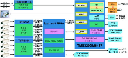
Figure 1 DSP + FPGA multi-channel video surveillance system hardware platform
16-bit video data bus · Up to 75MHz pixel clock frequency
·Can directly interface CCD or CMOS image sensor ·Can interface 8/10 bit BT.656 standard digital video stream ·Can interface 8/16 bit YCbCr 4:2:2 format digital video stream with line and field synchronization signal 
Figure 2 Block diagram of the 4-channel video decoder TVP5154
Receive/buffer 8 8-bit BT.656 digital video input data (pixel clock is 27MHz)
· Each channel is reduced by 1/2 horizontally/vertically, reduced from D1 format to CIF format · Splicing 8 CIF format digital videos into one 8-bit, 54MHz, YCbCr 4:2:2 band, field synchronization Digital video stream to video front-end VPFE of interface DM6437 
Fig. 3 Spartan-3 series FPGA structure
Analog video input: 8 standard PAL/NTSC analog video inputs, composite video CVBS, super video Y/C
Analog Video Output: 1 standard PAL/NTSC analog video output, composite video CVBS, super video Y/C, or component video YPbPr or RGB for local preview or test
· Video Decoder: 2 TVP5154s accept 8 channels of standard analog video input, 8 channels of 8 bit BT.656 digital video stream output · Input port: standard analog video input, composite video CVBS, or super video Y/C
· Data port: 8-bit data line, clock SCLK, line/field synchronization control signals HSYNC, VSYNC, FID, etc. · Control port: IIC bus, used to set the video decoder operating parameters and feedback status information · Video encoder: Directly by TMS320DM6437 on-chip video processing back-end implementation of a standard analog video output CVBS, or S-Video, or component video
Video Processing Front-end VPFE
16-bit data: CI[7:0]/CCD[15:8], YI[7:0]/CCD[7:0]
·Synchronization signals: pixel clock, line synchronization, frame synchronization, field flag · Video processing back-end VPBE
Analog Video Interface: Composite Video CVBS, or Super Video Y/C, or Component Video YPbPr/RGB
Digital video interface: 24-bit data, line/field synchronization signals, etc.
Receive/buffer eight 8-bit BT.656 digital video streams from the video decoder (pixel clock is 27MHz)
· Each channel is reduced by 1/2 horizontally/vertically, and the D1 format image is reduced to the CIF format image · The 8-channel CIF format digital video data is spliced ​​into a 8-bit, 54 MHz, D1 format digital video data stream. Interface DM6437 Video Processing Front-end VPFE
Can be set by software to select one channel of D1 format video data among 8 channels of video input, and 8 channels of EMIFA bus of interface DM6437 for preview
· The DM6437 video front-end VPFE is configured as an 8-bit, 54-MHz digital video port that implements 8-channel CIF format video input. · The DM6437 video back-end VPBE is configured as an analog video output that directly drives the monitor. 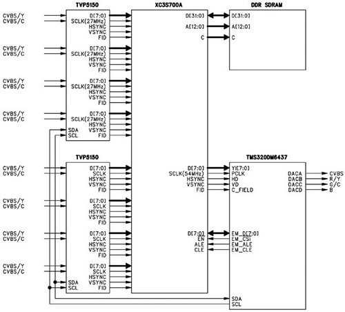
DSP+FPGA embedded multi-channel video monitoring system hardware platform
In recent years, especially after 9/11, the demand for video surveillance on various occasions has been growing, and at the same time it may be necessary to monitor multiple targets at the same time. This gives us the requirement to reduce the cost of single-channel video processing as much as possible. Performing as many digital video compression processes as possible with a single DSP processor will undoubtedly be an effective way to reduce the cost of single-channel video surveillance. Fortunately, with the continuous improvement of DSP processing performance, and the further optimization and maturity of embedded digital video codec algorithms, it has become possible to perform digital video compression processing of up to eight channels of CIF format by a single DSP. This article uses a TMS320DM6437 from TI's latest Davinci series DSP and Xilinx's high-performance, low-cost Spartan-3 series FPGA to build a high-performance, low-cost embedded multi-channel video surveillance system hardware platform.