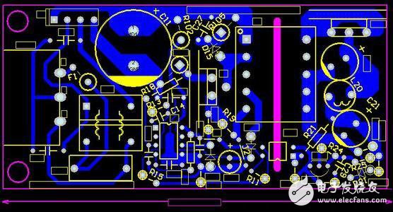
Surgery is very important, and postoperative recovery is also essential! After the various PCB layouts are completed, is it ok? Obviously, no! After the PCB wiring inspection work is also very necessary, then how to check the wiring in the PCB design, paving the way for the subsequent PCB design, circuit design? This article will teach you how to complete the inspection after PCB wiring from the various characteristics of PCB design, and do the final check! Before explaining the inspection work after the PCB layout is completed, we will introduce the special wiring skills of the three PCBs. The PCB LAYOUT trace will be explained from three aspects: right angle trace, differential trace, and serpentine line: First, right angle routing (three aspects) The effect of the right-angled trace on the signal is mainly reflected in three aspects: First, the corner can be equivalent to the capacitive load on the transmission line, slowing down the rise time; second, the impedance discontinuity will cause the signal to reflect; third, the right-angle tip is generated. EMI, to the RF design field above 10GHz, these small right angles may become the focus of high-speed problems. Second, the differential trace ("equal length, equidistance, reference plane") What is the differential signal (DifferenTIal Signal)? In layman's terms, the driver sends two equal-valued, inverted signals. The receiver compares the difference between the two voltages to determine whether the logic state is "0" or "1". The pair of traces carrying the differential signals is called a differential trace. Compared with ordinary single-ended signal traces, the most obvious advantages of differential signals are reflected in the following three aspects: 1. Strong anti-interference ability, because the coupling between the two differential traces is very good. When there is noise interference from the outside, it is almost simultaneously coupled to two lines, and the receiving end only cares about the difference between the two signals. Therefore, the common mode noise of the outside world can be completely offset. 2, can effectively suppress EMI, the same reason, because the polarity of the two signals is opposite, their external electromagnetic field can cancel each other, the closer the coupling, the less electromagnetic energy vented to the outside. 3. Timing positioning is accurate. Since the switching change of the differential signal is located at the intersection of the two signals, unlike the ordinary single-ended signal, which depends on the high and low threshold voltages, it is less affected by the process and temperature, and can reduce the timing error. It is also more suitable for circuits with low amplitude signals. The currently popular LVDS (low voltage differenTIal signaling) refers to this small amplitude differential signaling technique. Third, the snake line (adjustment delay) Serpentine lines are a type of routing that is often used in Layout. Its main purpose is to adjust the delay and meet the system timing design requirements. The two most important parameters are the parallel coupling length (Lp) and the coupling distance (S). It is obvious that when the signal is transmitted on the serpentine trace, the coupling between the parallel segments will occur in the form of differential mode. The smaller the Lp, the greater the degree of coupling. It may cause a reduction in transmission delay and greatly reduce the quality of the signal due to crosstalk. The mechanism can be referred to the analysis of common mode and differential mode crosstalk. Here are some suggestions for dealing with Python engineers when dealing with snake lines: 1. Try to increase the distance (S) of the parallel line segment, at least greater than 3H. H refers to the distance from the signal to the reference plane. In layman's terms, it is to follow the big bend line. As long as S is large enough, the mutual coupling effect can be almost completely avoided. 2. Reduce the coupling length Lp. When twice the Lp delay approaches or exceeds the signal rise time, the resulting crosstalk will reach saturation. 3. The stripe line of the Strip-Line or Embedded Micro-strip causes less signal transmission delay than the Micro-strip. In theory, the stripline does not affect the transmission rate due to differential mode crosstalk. 4, high-speed and signal lines with stricter timing requirements, try not to take the serpentine line, especially in the small range. 5, can often use snake-shaped lines at any angle, can effectively reduce the coupling between each other. 6. In high-speed PCB design, the serpentine line has no so-called filtering or anti-interference ability, and it can only reduce the signal quality, so it is only used for timing matching and has no other purpose. 7. Sometimes the winding can be considered in the way of spiral routing. The simulation shows that the effect is better than the normal serpentine routing. Surgery is very important, and postoperative recovery is also essential! After finishing the PCB layout, is it finished? Obviously, no! Post-PCB inspection is also necessary, so how to check the wiring in the PCB design, paving the way for later design? Please see below! General PCB design inspection project 1) Has the circuit been analyzed? In order to smooth the signal circuit into basic units? 2) Does the circuit allow for short or isolated key leads? 3) Is the place that must be shielded effectively shielded? 4) Make full use of the basic grid graphics? 5) Is the size of the printed circuit board the best size? 6) Is the selected wire width and spacing as much as possible? 7) Is the preferred pad size and hole size used? 8) Is the photographic plate and sketch suitable? 9) Is the minimum number of jumpers used? Do jumpers pass through components and accessories? L0) Can the letters be seen after assembly? Is the size and model correct? 11) In order to prevent foaming, does the large area of ​​copper foil open the window? 12) Is there a tool positioning hole? PCB electrical characteristics inspection items: 1) Have you analyzed the effects of wire resistance, inductance, and capacitance? Especially the impact of the critical pressure drop on the ground? 2) Does the spacing and shape of the wire accessories meet the insulation requirements? 3) Is the insulation resistance value controlled and specified at the critical point? 4) Is the polarity fully recognized? 5) From the geometric point of view, the influence of the wire spacing on the leakage resistance and voltage is measured? 6) Has the medium that changed the surface coating been identified? PCB physical property inspection project: 1) Are all pads and their locations suitable for final assembly? 2) Can the assembled printed circuit board meet the shock and vibration conditions? 3) What is the spacing of the specified standard components? 4) Are the components that are not securely mounted or the heavier parts fixed? 5) Is the heat-dissipating component of the heating element cooled correctly? Or is it isolated from printed circuit boards and other thermal components? 6) Is the voltage divider and other multi-lead components positioned correctly? 7) Is the component arrangement and orientation easy to check? 8) Have all possible interferences on the printed circuit board and the entire printed circuit board assembly been eliminated? 9) Is the positioning hole the correct size? 10) Is the tolerance complete and reasonable? 11) Have you controlled and signed the physical properties of all coatings? 12) Is the hole and lead diameter ratio within the acceptable range of public energy? PCB mechanical design factors: Although the printed circuit board uses mechanical means to support the component, it cannot be used as a structural member of the entire device. In the edge of the printed version, at least every 5 inches for a certain amount of text. The factors that must be considered when selecting and designing a printed circuit board are as follows; 1) The structure of the printed circuit board - size and shape. 2) Type of mechanical attachment and plug (seat) required. 3) Adaptability of the circuit to other circuits and environmental conditions. 4) Consider installing the printed circuit board vertically or horizontally depending on factors such as heat and dust. 5) Some environmental factors that require special attention, such as heat dissipation, ventilation, shock, vibration, and humidity. Dust, salt spray and radiation. 6) The extent of support. 7) Keep and fix. 8) Easy to take down. Die-Casting Products,Led Housing Die Casting,Aluminum Die Casting Product,Aluminum Die Casting Led Yangzhou Huadong Can Illuminations Mould Manufactory Co., Ltd. , https://www.light-reflectors.com