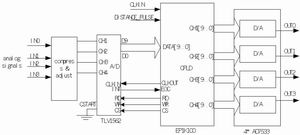
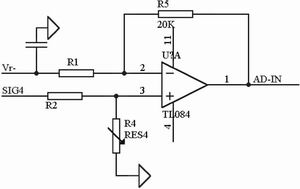
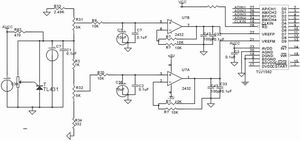
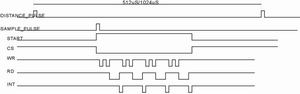
Pick   To:       This paper presents a design and implementation of a 4- channel real-time data acquisition and processing system based on TLV1562 . This system is applied to the radar real-time adaptive noise canceller, which can meet the requirements of real-time radar signal cancellation and has a good effect. introduction In the design of radar clutter cancellers, the traditional method is to use intermediate frequency cancellation, that is, the suppression of clutter is achieved at the intermediate frequency. Early intermediate frequency cancellers often used analog delay lines such as SAW and CCD . Due to the outstanding advantages of digital signal processing , especially the development of digital integrated circuits and the increasingly powerful functions of programmable logic devices , digital vector cancellers have become the main working mode at present and in the future. The acquisition and processing of radar signals have become the most critical link. In the design, the author chose 10 -bit high-speed low-power reconfigurable TLV1562 to achieve multi-channel data acquisition and processing at a lower cost. System design and implementation The system block diagram is shown in Figure 1. The front-end acquisition system with TLV1562 as the core is part of the entire system. The entire system consists of signal conditioning, signal sampling, high-speed signal processing ( digital cancellation ) and waveform playback. The signal conditioning circuit is to compress and adjust the signal sent by coherent detection to meet the sampling level of TLV1562 ; signal sampling is to complete the digitization of analog signals ( completed by TLV1562 ) ; high-speed digital signal processing is to complete digital cancellation in CPLD Algorithm; the waveform playback part formed by AD7533 is to send the processed signal to the display screen. Signal conditioning circuit and A / D reference source Since for the AVDD predetermined supply voltage, the analog input signal range is TLV1562 0.8V (AVDD-1.9 volts), the analog signal must be carried out coherent detection processing, to meet the requirements. Design, using conditioning circuit shown in Figure 2, R4 for adjusting the amplitude of the input signal range of SIG4, Vr- adjust TL431 out by a reference voltage for the DC voltage control signal. TLV1562 has two reference input pins- REFP and REFM . The levels on these two pins are the upper and lower limits of the analog input that produces full-scale and zero-degree readings, respectively. According to the requirements, the reference voltage must meet the following conditions: VREFP <= AVDD-1V AGND + 0.9V 3V> = (VREFP-VREFM)> = 0.8V Therefore, the reference design shown in Figure 3 is used in the design. By adjusting R31 and R32 , VREFP and VREFM meet the appeal requirements. Acquisition System The timing diagram of the interface between CPLD and TLV1562 is shown in Figure 4 . DISTANCE_PULSE distance gate pulse period is 512 μ s (80Km) or 1024 μ s (160Km), SAMPLE_PULSE sampling start pulse, its rising edge of acquisition once the monitoring system is started, the START is set high, TLV1562 of CS is set low. The timing diagrams of WR , RD , and INT are the timing diagrams of the internal conversion mode of TLV1562 . When WR appears low twice, the configuration of registers CR0 and CR1 is completed, that is , the initialization of A / D conversion is realized . The A / D conversion ends, the output low-level signal INT is valid, the signal RD reads the A / D conversion result and resets the INT signal, completes a conversion cycle, and starts preparing for the next conversion. Since the TLV1562 chip is a configurable A / D converter, it is one of the key technologies how to use CPLD to realize the configuration and reading and writing of the TLV1562 . The read and write control for TLV1562 is easy to implement, and for its configuration, it is more complicated because it is a four-channel cyclic acquisition. There are two registers in TLV1562 that need to be configured, that is, there are two writes, and the data for each configuration is not the same, so the data should be provided accordingly during each write. The entire configuration process is implemented in VHDL language using finite state machine. Define 5 states: st0 , st1 , st2 , st3 , st4 , st0 are idle state, st1 , st2 , st3 , st4 are corresponding to the corresponding acquisition channel state, INDEXREG [1..0] is used to monitor the write signal An identification code written several times. The procedure is as follows: type states is (st0, st1, st2, st3 , ST4); signal current_state, next_state: states: = st0; signal indexreg: STD_LOGIC_vector (1 downto 0);   signal chanel_data: STD_LOGIC_vector (9 downto 0); begin indexreg <= index_reg; cs <= not start; process (current_state, indexreg, ad_ale) begin   if ad_ale = '0' then      chanel_data <= "ZZZZZZZZZZ"; else    if indexreg = "10" then    chanel_data <= "0100000100";  else case current_state is     when st0 => ad_end <= '0'; chanel <= "00";               next_state <= st1;               chanel_data <= "0011000000";     when st1 => ad_end <= '0'; chanel <= "01";               next_state <= st2;               chanel_data <= "0011000001";     when st2 => ad_end <= '0'; chanel <= "10";                next_state <= st3;               chanel_data <= "0011000010";     when st3 => ad_end <= '1'; chanel <= "11";                next_state <= st0;               chanel_data <= "0011000011";    when st4 => next_state <= st0;               chanel_data <= "0011000000";    when others => ad_end <= '1' ; next_state <= st0;               chanel_data <= "0011000000";   end case;  end if;  end if; end process; Conclusion The design and implementation method of multi-channel high-speed acquisition system based on TLV1562 and EP1K100 are detailed in this paper . The acquisition system is applied to radar digital canceller . Achieve multi-channel data acquisition and processing at a lower cost. ■references: 1. TLV1562 USER GUIDE, TI Co.US, 1999. 2. HIGH-SPEED LOW-POWER RECONFIGURAB-LE ANALOG-TO-DIGITAL TLV1562. Figure 1 Block diagram of radar canceller system Picture 2  Signal conditioning circuit Picture 3  Reference circuit design Picture 4  Timing diagram of the interface between EP1K100 and TLV1562 Jilin Province Wanhe light Co.,Ltd , https://www.wanhelight.com