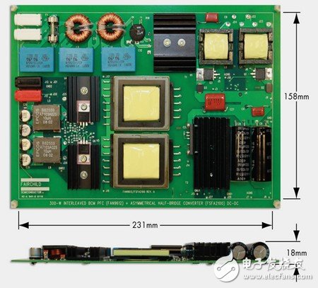
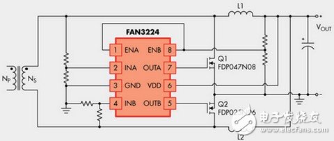
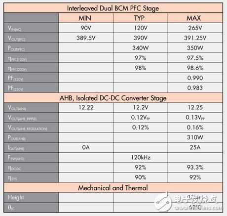
Even for the most experienced power supply designers, maximizing power efficiency in a small footprint is not an easy task. There are many devices that require a small power supply design, and such devices may need to provide hundreds of watts of power to the load at a given time. For systems with a height limit of less than 1U, forced air cooling may not be feasible, which means that a costly large surface area thin heat sink must be used for thermal management. The AC/DC power supply is a power module whose input is AC and the output is DC. Among them, the module includes a rectification filter circuit, a step-down circuit and a voltage stabilization circuit. In the AC/DC power conversion application, a wide input range is required. Usually, the AC input of 85V~265V is required, the output power conversion efficiency is high, and the energy saving performance can be effectively improved. The full load efficiency is designed in the AC/DC power supply. Medium is a major consideration. The method of improving the efficiency of AC/DC converters and achieving better energy-saving performance is the advocacy of green energy. In most cases, AC-DC power supplies operating at these power levels require some type of active power factor correction (PFC). The power semiconductors are soldered directly to the PCB and then pasted onto the chassis instead of being insulated and bolted to the chassis. Considering the cost of the heat-bonding material, the overall assembly cost will decrease. This also reduces the size of the power supply and reduces the temperature at the device connection by approximately 10 degrees Celsius, thereby doubling the mean time between failures. For AC-DC power supplies, a non-isolated off-line boost pre-converter is typically used as the PFC stage with its DC output voltage as the input to the downstream isolated DC-DC converter. Since the two converters are connected in series, the overall system efficiency ηSYS is the product of the efficiency of each converter: It is obvious from equation (1) that a system solution with many high-efficiency characteristics is combined with an interleaved double critical conduction mode (BCM) PFC and an isolated DC-DC converter, wherein the former is followed by an asymmetric half bridge (AHB). The latter uses a secondary side of a double current rectifier with a self-driven synchronous rectifier. Figure 1.12V, 300W, small universal AC-DC power supply. For PFC converters in the 300W-1kW range, the Interleaved Critical Conduction Mode (BCM) PFC should be considered because it is more efficient than the Continuous Conduction Mode (CCM) PFC control technique at similar power levels. Interleaved BCM PFC is based on a variable frequency control algorithm in which two PFC boost power stages are 180 degrees out of phase with each other. Due to the effective inductor ripple current cancellation, the high peak currents common in EMI filters and PFC output capacitors are reduced. The output PFC bulk capacitor benefits from ripple current cancellation because the AC RMS current flowing through the equivalent series resistance (ESR) is reduced. In addition, since the boost MOSFET is turned off under the zero-voltage switch (ZVS) depending on the AC line and turned on under the zero current switch (ZCS), the efficiency can be further improved. For a 350W interleaved BCM PFC design, the MOSFET heat sink can be removed, as shown in Figure 1. On the other hand, the boost MOSFET used in the CCM PFC design is susceptible to frequency-dependent switching losses, which are proportional to the input current and line voltage. By turning off the interleaved BCM boost diodes at zero current, reverse recovery losses are avoided, allowing the use of low-cost, fast-recovery rectifier diodes and, in some cases, no heat sinks. The inherent characteristics of the PFC converter are: when the output voltage is regulated by voltage type PWM control, the steady-state duty ratio Du is constant (that is, the on-time Ton is constant), and the input current is close to a sine wave. Therefore, power factor correction can be achieved without multipliers and current control in the control circuit. For isolated dc-to-dc converter designs, the half-bridge is a good topological choice because it has two complementary-drive primary-side MOSFETs and the maximum drain-to-source voltage is limited by the applied DC input voltage. LLC implements ZVS through variable frequency control techniques using parasitic elements associated with power level design. However, since the regulated DC output uses only capacitive filtering, this topology is best suited for applications with lower output ripple and higher output voltage. AHB is mainly used for connection between high-performance modules (such as CPU, DMA and DSP). As the SoC's system-on-chip bus, it includes the following features: single clock edge operation; non-tri-state implementation; support for burst transmission Support segmented transfer; support multiple host controllers; configurable 32-bit to 128-bit bus width; support for byte, nibble, and word transfers. The AHB system consists of three parts: the main module, the slave module and the infrastructure AHBInfrastructure. The transmission on the entire AHB bus is sent by the main module, and the slave module is responsible for responding. The infrastructure consists of the arbiter, the multiplexer of the master module to the slave module, the multiplexer of the slave module to the master module, the decoder, the dummy slave, and the dummy master. composition. For 300W, 12V DC-DC converters, AHB is an efficient choice. Since the primary current lags the primary voltage of the transformer, it provides the necessary conditions for the ZVS of the two primary MOSFETs. Similar to LLC, the ability to implement ZVS with AHB also depends on a thorough understanding of the parasitic elements of the circuit, such as transformer leakage inductance, turn-to-turn capacitance, and junction capacitance of discrete devices. Compared to the variable frequency control method used in LLC control, the fixed frequency scheme can greatly simplify the task of the secondary side self-driven synchronous rectification (SR). The gate drive voltage of the self-driving SR is easily derived from the secondary side of the transformer. Adding a low-side MOSFET driver, such as the dual 4A FAN3224 driver shown in Figure 2, gives accurate level shifting and high peak drive current through the MOSFST Miller flat region. Figure 2. FAN3224, self-driven synchronous rectification (SR) with a double current rectifier. This double current rectifier can be used in any double-ended power supply topology and large DC current applications with several outstanding features. First, its secondary side consists of a simple winding that simplifies the transformer construction. Second, since the required output inductance is distributed across the two inductors, the power dissipation due to the large current flowing into the secondary side is more effectively distributed. Third, as a function of duty cycle (D), the two inductor ripple currents cancel each other out. The sum of the two inductor currents offset is twice the apparent frequency of the switching frequency, allowing for higher frequencies and lower peak current into the output inductor. The voltage asymmetry applied to the secondary side rectifier may be one of the disadvantages of AHB. When the AHB is operating near its limit D = 0.5, the loaded SR voltage can almost reach a match. However, a more reasonable solution is to keep D at 0.25 during rated operation by designing the turns ratio of the transformer. The regulator is followed by an asymmetric half-bridge DC-DC converter with self-driving SR, as shown in Figure 1. Table 1. Small AC-DC Power Supply Design Specifications The specifications in Table 1 are a brief summary of all design requirements. The main design objectives are as follows: 1. Get maximum efficiency over the widest possible range. 2. Achieve the smallest possible design size. 3. The use and size of the heat sink is minimized. Single Burner Electric Hotplate Portable Hot Plate,Single Burner Electric Hotplate,Hot Plates,Hot Plates With Stainless Housing Shaoxing Haoda Electrical Appliance Co.,Ltd , https://www.zjhaoda.com![]() (1)
(1)